 | –≠–Ľ–Ķ–ļ—ā—Ä–ĺ–Ĺ–Ĺ—č–Ļ –ļ–ĺ–ľ–Ņ–ĺ–Ĺ–Ķ–Ĺ—ā: CPCI-511 | –°–ļ–į—á–į—ā—Ć:  PDF PDF  ZIP ZIP |
FEATURES
∑
High precision 16-bit A/D resolution
∑
Sample rates up to 100 KHz
∑
32 single-ended or 16 differential A/D channels
∑
Software programmable gain amplifier (PGA) gain/
channel memory
∑
Signal conditioning pads for each analog input
∑
On-board FIFO stores up to 512 A/D samples
∑
Pulse rate, pulse period, and event counting
∑
Programmable timebase and square wave generation
∑
Supplies precision, adjustable transducer excitation
∑
Two 16-bit D/A voltage and 4-20 mA current outputs
∑
24 digital inputs and outputs
∑
CompactPCI bus interface supports DMA and plug and
play (PnP)
∑
Pentium
ģ
and Windows
ģ
95/98/NT/2K compatible
GENERAL DESCRIPTION
Harness and exploit the power of the CompactPCI bus with this low
cost solution to all your test, measurement, and control
applications. The CPCI-511 combines analog input, analog output,
digital input/output (I/O), and counter/timer I/O on a CompactPCI
plug-in board that is designed for intelligent, high precision data
acquisition and process control. It is particularly suited to a host of
sensor and transducer inputs, such as strain gauges, RTD's, bridge
circuits, and displacement sensing elements, as well as strip chart
recording , and multi-channel data logging in factory automation,
research labs, and industrial control.
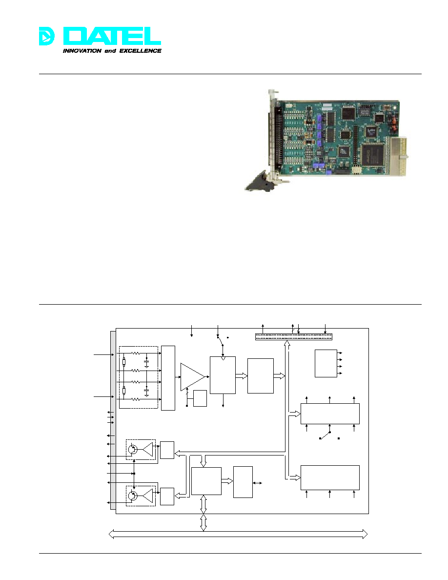
Figure 1. CPCI-511 Functional Block Diagram
Using the latest data conversion technology, the CPCI-511
combines many of the features usually provided in expensive stand
alone data acquisition systems with significant savings. Numerous
external signal conditioning modules are available to accommodate
various sensor input requirements such as channel isolation,
current inputs, and relay switching. The PCI bus plug and play
(PnP) interface enables PC auto-detection and initialization, and
eliminates all user hardware configuration. Simply plug the board
into your computer, install DATEL's CPCI-511WIN software, and
within minutes you will be analyzing and displaying data in real
time, or archiving that data onto hard disk for later processing.
CPCI-511
Precision Sensor Input and Multi-Function
I/O Board for CompactPCI bus
DATEL, Inc., Mansfield, MA 02048 (USA)
∑
Tel: (508)339-3000, (800)233-2765 Fax: (508)339-6356
∑
Email: sales@datel.com
∑
Internet: www.datel.com
ģ
ģ
Rate Generator Out
PulseRate/Period In
Ext. Event Clock In
External A/D
Trigger In
Analog Inputs
+10V Out
+5V, 0.75A Fused
4-20 mA Current
Loop Output
DAC V Out 0
Current Loop
Excitation In
DAC V Out 1
4-20 mA Current
Loop Output
M
U
X
2 k
2 k
Signal Conditioning Pad
Software
PGA
PGA Gain
Control
x1, x2, x5, x10
+
≠
16 bit
DAC
4-20 mA Current Loop
+
≠
16 bit
DAC
4-20 mA Current Loop
AMCC S5933
PCI bus
Controller
16-bit
100 kHz
A/D
Converter
512
Sample
FIFO
82C54 Timer
A/D Control
Address
Decode
Logic
Register
Controls
24 Digital
I/O
Data Clock
Input
+5V
Fused 0.75A
End of Conversion
(EOC)
A/D Start Clock
Internal
A/D Clock
External A/D
Clock In
Local Data Bus
CompactPCI Bus
A/D
Clock
A/D
Trigger
A/D Sample
Trigger Count
1 MHz
1 MHz
100 KHz
82C54 Timer
General Purpose
Rate Generator
Event Counter
Period/Frequency Measurement
10 MHz
Ext.
Event
Clock
Control
Signals
EOC
2 k
2 k
R
OPT
C
OPT
R
OPT
C
OPT
Voltage
Reference
and
Temp.
Sensor
+10V
+2.5V
+3.3V
Temp.
Sensor Out
Gain/
Chan
Mem
33
PRODUCT DATA

CPCI-511
ģ
ģ
DATEL, Inc., Mansfield, MA 02048 (USA)
∑
Tel: (508)339-3000, (800)233-2765 Fax: (508)339-6356
∑
Email: sales@datel.com
∑
Internet: www.datel.com
The CPCI-511 offers 32 single-ended analog inputs that are
software configurable as 16 true differential inputs. The full
scale input voltage range is Ī10V. Each input channel includes
blank component pads that are user-configurable to accept
different input voltage ranges, current inputs, simple filters, or
other signal conditioning. A software programmable gain
amplifier (PGA) offers high input signal gains that allow the
board to detect low level sensor inputs. The A/D resolution is 16
bits, and it can sample at up to 100 thousand times per second.
Channels can be individually sampled, or a software selectable
group of adjacent channels can be scanned continuously.
Analog Input Gain Channel Memory
The on-board gain/channel memory stores PGA gain codes for
each analog input channel. After loading the gains for all the
channels, the CPCI-511 may be software selected to
automatically load the Programmable Gain Amplifier with the
desired code before each sample. In either case, the user must
allow adequate PGA settling time before starting the next sample.
Automatic Input Channel Address Sequencing
The CPCI-511 includes registers for the start and final analog
input channel addresses. After loading these registers, the board
may be selected to automatically advance the channel address
after each A/D conversion. When the final channel is reached,
the system reloads the start channel for continuous automated
sequencing. This produces a series of sequential A/D samples in
the FIFO memory. The Command Register will also lock the
address on a single channel for repeated sampling.
This autoincrement channel addressing may be combined with
the gain/channel memory feature and the A/D FIFO memory to
achieve mostly unattended automatic sampling of thousands
of samples. The host program merely has to retrieve blocks of
data periodically.
A/D data passes directly to an on-board first-in-first-out (FIFO)
memory. This architecture allows non-stop, continuous data
streaming to the computer without losing any samples. The
streaming mode uses high speed PCI bus mastering (also
known as Direct Memory Access - DMA) to place the data
directly into host memory without CPU intervention. This frees
up host CPU processing time, allowing it to perform other
concurrent tasks such as data analysis, data display, and
process control. Slower speed applications can use the FIFO
to store up to 512 samples. Synchronization provided by
software detectable FIFO flags (full, half full, and empty), and
an end of trigger frame indicator, enable the host to
periodically read one or all stored samples, and then return to
other simultaneous tasks until more data is ready.
The A/D sampling rate is software selectable using an on-
board 82C54 timer. The timer allows software programmable
sampling rates from the maximum A/D speed of 100 KHz all
the way down to 15.25 Hz. A/D sampling can also be directly
controlled by a user-supplied external clock input. An internal
programmable trigger timer allows acquisition of blocks of
samples separated by programmable delays. In addition,
external digital triggers can be used. For application
synchronization and event detection, a programmable sample
counter specifies the number of samples per trigger frame,
which is independent of FIFO size and PCI bus transfer
counts. This flexible timing architecture makes the CPCI-511
an ideal solution for most medium speed electronic test,
measurement, instrumentation, and control applications.
A second programmable counter/timer accommodates pulse
rate (frequency) and period measurements, event counting,
clock and timebase generation, square wave generation, and
other general timing applications. An on-board, precision 10
MHz oscillator is used as the timebase for timing and wave
generation. Digital pulse trains can be generated at pre-
programmed rates and software selectable pulse widths for logic
testing and simulation. Externally supplied inputs allow period
and frequency measurements, as well as event counting.
The CPCI-511 provides voltage and current excitation outputs
for RTD's and strain gauges. The strain gauge voltage output is
a regulated +10V (100 mA max.) source, while the RTD current
source output is fixed at 500ĶA (Ī2% nominal). To verify strain
gauge voltages and RTD currents these excitation outputs can
be steered by software to the analog inputs. Other on-board
software selectable A/D input sources include 5V fixed
references and both D/A channels. An on-board temperature
transducer uses a precision bandgap voltage reference to
provide an output voltage that varies linearly with temperature.
This temperature sensor can be selected as an A/D input for
reference temperature compensation for RTD's.
The CPCI-511 includes two 16-bit digital to analog converters
(DAC's) that add precision adjustable voltage and current
outputs for transducer excitation, process control, and
programmable voltage sources. The full scale output voltage
range is Ī10V, at 5 mA maximum per channel. Each DAC
channel drives an on-board 4-20 mA current loop. The
excitation power for the current loop is user-selectable from an
internal 12V reference or from an external 12V to 30V supply.
User supplied excitation allows higher impedance loads to be
connected while still maintaining current loop voltage
compliance. Gain and offset adjustment potentiometers are
provided on each DAC channel for precision calibration. Under
software control, the DAC outputs can drive the analog inputs
for A/D and PGA calibration.
The CPCI-511 also provides 24 digital inputs and outputs for
discrete monitoring and control systems, inter-machine
communication, digital pattern recognition, digital signature
generation, and relay switching applications. All the lines are
TTL and CMOS compatible. The output port latches the data
when commanded by host software. A user-supplied strobe
latches data at the input port for reading by host software. The
digital lines are accessed via the front panel connector which
also supplies +5V and ground for external circuits. Various
transition panels allow direct connection to industry standard
interfaces such as Opto 22 modules.
The CPCI-511 is built on a 3U CompactPCI board that occupies
one CompactPCI slot. The product is manufactured in DATEL's
ISO9001 facility. The PCI bus interface is implemented using an
AMCC S5933 PCI bus controller that supports full PCI bus
mastering.
34
CPCI-511
ģ
ģ
DATEL, Inc., Mansfield, MA 02048 (USA)
∑
Tel: (508)339-3000, (800)233-2765 Fax: (508)339-6356
∑
Email: sales@datel.com
∑
Internet: www.datel.com
CPCI-511WIN(S) Software
Windows
ģ
95/98/NT/2K have become the platforms of choice for
many data acquisition, test, measurement, and control
applications. These feature-rich, 32-bit operating systems exploit
huge gigabyte memory, secure multi-threading, and hardware
plug-and-play (PnP) to provide high performing, user friendly
working environments. CPCI-511WIN is an interactive data
acquisition, analysis, display, signal generation, and digital I/O
software system for the CPCI-511 that runs under Windows
ģ
95/
98/NT/2K. It consists of a point-and-click graphic user interface
(GUI), a dynamic link library (DLL), and a device driver.
CPCI-511WIN main features include:
∑
Plug and Play (PnP) hardware detection and initialization.
∑
Easy-to-use, point and click graphic user interface (GUI).
∑
Transparent A/D data transfer to host memory using DMA.
∑
Control multiple CPCI-511's in the same computer
simultaneously.
∑
A/D configuration ≠ PGA gain, sample rate, etc.
∑
Set the DAC voltage and 4-20 mA current outputs.
∑
Read and write the digital I/O ports.
∑
Event counting, period, and frequency measurements.
∑
Generate digital signals, program pulse rates and widths.
CPCI-511WIN automatically detects the CPCI-511, configures
the hardware, and continuously streams A/D sensor data to
host memory using PCI bus DMA. A/D selections such as
single-ended/differential, PGA gain, sample rate, trigger rate,
and channel scan groups can be selected with the mouse.
Generate dynamic voltage waveforms or DC levels from both
DAC voltage and 4-20 mA outputs. Read and write the digital
I/O ports on command, or transfer blocks of data to and from
the ports for pattern recognition, digital signature generation,
and control. Timer control and manipulation selections perform
event counting, pulse rate measurement, and pulse
generation. The raw data can be displayed in decimal or hex,
with real time scrolling.
CPCI-511WIN turns your computer into an intelligent data
logger, archiving all A/D sensor data to disk for later analysis
using third party applications such as Excel
ģ
and LabVIEW
ģ
.
Analog and digital channel expansion can be achieved by
running multiple CPCI-511's in the same computer
simultaneously. Multiple, concurrent real time displays can be
viewed, and the data from each board can be logged to
separate disk files for later analysis.
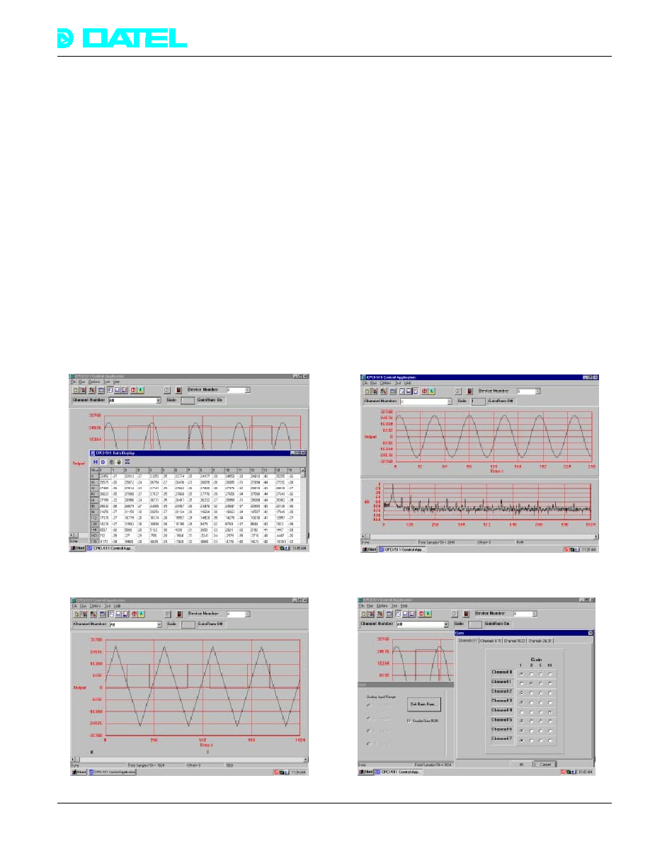
Figure 2. CPCI-511WIN with Data Table
Figure 4. CPCI-511WIN FFT Display
35
Figure 3. CPCI-511WIN Two Channel Display
Figure 5. CPCI-511WIN Gain RAM Selection

CPCI-511
ģ
ģ
DATEL, Inc., Mansfield, MA 02048 (USA)
∑
Tel: (508)339-3000, (800)233-2765 Fax: (508)339-6356
∑
Email: sales@datel.com
∑
Internet: www.datel.com
Software engineers and programmers will be interested in
CPCI-511WINS -- the source code for CPCI-511WIN. It
includes complete source code for the GUI (Borland C
++
Builder) and the DLL (Visual C
++
5.0), and allows you to
communicate with the CPCI-511 from the familiar environment
of your favorite high level language ≠ C, Visual
ģ
BASIC, etc. It's
standard Windows programming hierarchy facilitates custom
software development and CPCI-511 integration into other
applications. The source code contains a simple example
console program, written in C, that exercises the CPCI-511
through DLL function calls.
CPCI-511WINS hardware register access includes:
Command Register
Controls for A/D trigger/clock selections, channel sequencing,
single-ended or differential input configuration, PGA gain
selections, and A/D calibration.
Status Register
FIFO flags (empty, half full, and full), counter/timer status, and
channel block scan complete.
Start Channel Register
Select the first A/D channel in a contiguous, sequential group
to scan. Channel addressing can be selected to automatically
increment after each sample.
Final Channel Register
Select the last A/D channel in a contiguous, sequential group
to scan.
Reset FIFO
Flush all FIFO data. All previous data not saved will be lost.
A/D Data Register
Read blocks of A/D data.
Interrupt Source / 82C54 Timer Control Register
Select counter/time mode (rate generator, event counter,
period, or frequency measurement), and non-DMA host
interrupt mode (FIFO full, half full, empty, end of trigger block).
Digital I/O Registers
Access the 82C55 I/O controller.
Write DAC 0 Register
Update the 16-bit analog output (channel 0).
Write DAC 1 Register
Update the 16-bit analog output (channel 1).
Write Gain/Channel Memory Register
Timer Control Registers
Configure both 82C54 timers.
Timer Data Registers
Load 82C54 timer data.
PCI Control Registers
Read/write access to all the registers on the AMCC S5933 PCI
bus controller.
The hardware user manual contains detailed information on each
bit in all the CPCI-511 registers.
*For example, the sample rate per channel sampling 16
channels is 25 KHz/16 = 1.56 KHz/channel.
SPECIFICATIONS
(Typical @ +25įC, dynamic conditions, gain = 1, unless noted)
ANALOG INPUTS
Number of Input Channels
32 single-ended or 16
differential
Input Configuration
Non-isolated.
Standard Input Voltage Range
Ī10V, Ī5V, Ī2V, Ī1V. Per-
channel higher ranges are
possible by installing
attenuation resistors in the
blank component pads.
A/D Resolution
16 bits.
Single Channel Sample Rate
100 KHz (single channel).
Multi-channel Sample Rate
25 KHz aggregate (per
channel sample rate =
25 KHz/no. of chans.).*
A/D Output Data Coding
Two's complement, sign
extended to indicate polarity.
Programmable Gain
Software programmable --
x1, x2, x5 or x10.
Gain/Channel Memory
Stores gain codes for each
A/D channel. May be selected
to automatically load the stored
gain into the PGA before each
sample.
Input Impedance
10 M
, minimum.
Signal Conditioning
The board includes
unpopulated component pads
on each channel for user-
installation of current shunts,
attenuators, simple filters, etc.
Common Mode Voltage Range
Ī10 Volts
Common Mode Rejection
92 dB typical, DC to 60 Hz,
1 K
unbalance, gain=1.
Input Over-voltage
Ī12 Volts max., sustained no
damage, power on or off.
Diode clamp protection only.
A/D Adjustments
Gain and offset.
Addressing Modes
1. Single channel by random
addressing in software.
2. Short cycle addressing ≠
continuously sample a block
of adjacent channels
Integral Linearity (gain=1)
Ī4 LSB of full scale range.
Differential Linearity (gain=1)
Ī3 LSB of full scale range.
Full Scale Temp. Coefficient
Ī1 LSB per degree C.
Offset/Zero Temp. Coefficient
Ī1 LSB per degree C.
Total Harmonic Distortion
-80 dB (optimized 16K FFT,
2
nd
to 5
th
harmonics)
Analog Input Connector
100 pin high density
36
CPCI-511
ģ
ģ
DATEL, Inc., Mansfield, MA 02048 (USA)
∑
Tel: (508)339-3000, (800)233-2765 Fax: (508)339-6356
∑
Email: sales@datel.com
∑
Internet: www.datel.com
ANALOG OUTPUTS
Number of D/A Channels
Two, non-isolated
D/A Resolution
16 bits
Settling Time
Full Scale Step
10 Ķs (100 KHz) max.
Single Step
6 Ķs
Slew Rate
10V/Ķs.
Output Voltage Range
Ī10V per channel.
Output Current
(Voltage outputs)
Ī5 mA minimum per channel.
Output Impedance
0.1 Ohms.
Short Circuit Protection
Short circuit to ground.
Integral Linearity Error
Ī4 LSB's maximum.
Differential Linearity Error
Ī4 LSB's maximum.
D/A Calibration
Gain and offset adjust
potentiometers per channel.
Data Coding
2's complement binary
A/D Excitation
The D/A channels may be
software selected for voltage
excitation of the A/D channels
Current Loop Outputs
Each D/A channel drives a
4-20 mA active current loop.
Current Loop Excitation
Internal fixed +12V supply or
external user-supplied
excitation (12V to 30V).
Current Loop Compliance
12V to 30V, non-isolated.
RTD Current Excitation
RTD excitation is fixed at
500 ĶA, Ī2% typical. Under
software control the CPCI-511
can verify that the RTD
current is present by directing
this excitation output to the A/D.
Strain Gauge Excitation
10V regulated, Ī2%, 100 mA
max. current output. Under
software control the CPCI-511
can verify that strain gauge
voltage is present by directing
this reference output to the A/D.
Temperature Transducer
On-board bandgap voltage
source that varies linearly
with temperature. It has an
output voltage of 250 mV at
25įC, and a temperature
coefficient of 10 mV per įC.
A/D Sample Clock (82C54)
Internal software
programmable or external
TTL input.
A/D Frame Trigger
Internal software
programmable or external
TTL input.
A/D Sample Counter
Software programmable to
65535 samples. Can disable
in software for continuous,
non-stop sampling for long
periods.
A/D FIFO Memory
512 A/D samples
SENSOR EXCITATION OUTPUTS
A/D TIMING AND FIFO MEMORY
GENERAL PURPOSE COUNTER/TIMER
Input Functions
Pulse rate and period
measurement, and event
counting.
Output Functions
Clock, timebase, or square
wave generator.
Clock source
Internal 10 MHz crystal or
external input (10 MHz max.).
Gate source
Internal (software) or external.
Input/output levels
1 TTL load min. (output),
1 TTL-LS load max. (input).
Controller
Standard 82C54 timer.
Number of channels
24 I/O, arranged as three 8 bit
bidirectional ports or two
buffered 8 bit ports with
strobes and latches.
Controller
82C55
Logic Levels
TTL-CMOS compatible.
Input Voltage
Input LOW Voltage 0.8V max.
Input HIGH Voltage 2.0V min.
Input Leakage Current
1 ĶA
Output Voltage
Output HIGH 3.8 V min.
Output LOW 0.5 V max.
Output Drive Current
Output Low 2.5 mA (1 TTL load)
Connector
100 pin high density on front
panel.
Settling Time
350 ns
Operating Temp. Range
0 to +60įC
Storage Temperature Range
-25 to +85įC no thermal shock.
Relative Humidity
10% to 90%, non-condensing.
Altitude
0 to 10,000 feet. Forced
cooling required.
Warm-Up Period
10 minutes to rated accuracy.
Bus Interface
32-bit CompactPCI bus using
the AMCC S5933 controller.
PCI Bus Mastering (DMA)
Automatically included with
the AMCC S5933.
PCI Interrupt Sources
Non-DMA mode: A/D FIFO full,
FIFO half full, FIFO empty, and
end of trigger frame/block. DMA
Mode: DMA T/C
Local RAM
Board includes non-volatile
Random Access Memory to
initialize the PCI controller,
store calibration tables, and
other model specific information.
Mechanical Outline
3U CompactPCI board - 100 x
Dimensions
160 x 20.32 mm, 4 PH.
Occupies one slot.
Regulated DC Power
Supplied by the host PCI bus:
Required
+5Vdc @ 750mA max.,
500 mA typical
+12Vdc @ 250mA max.,
150 mA typical
-12Vdc @ 150mA max.,
100 mA typical
Manufacturing Environment
ISO 9001 certified facility.
DIGITAL INPUT/OUTPUT PORT
MISCELLANEOUS
ENVIRONMENTAL
37