DAC-HZ Series
12-Bit, Industry-Standard
Digital-to-Analog Converters
INNOVATION and EX C ELL E N C E
ģ
ģ
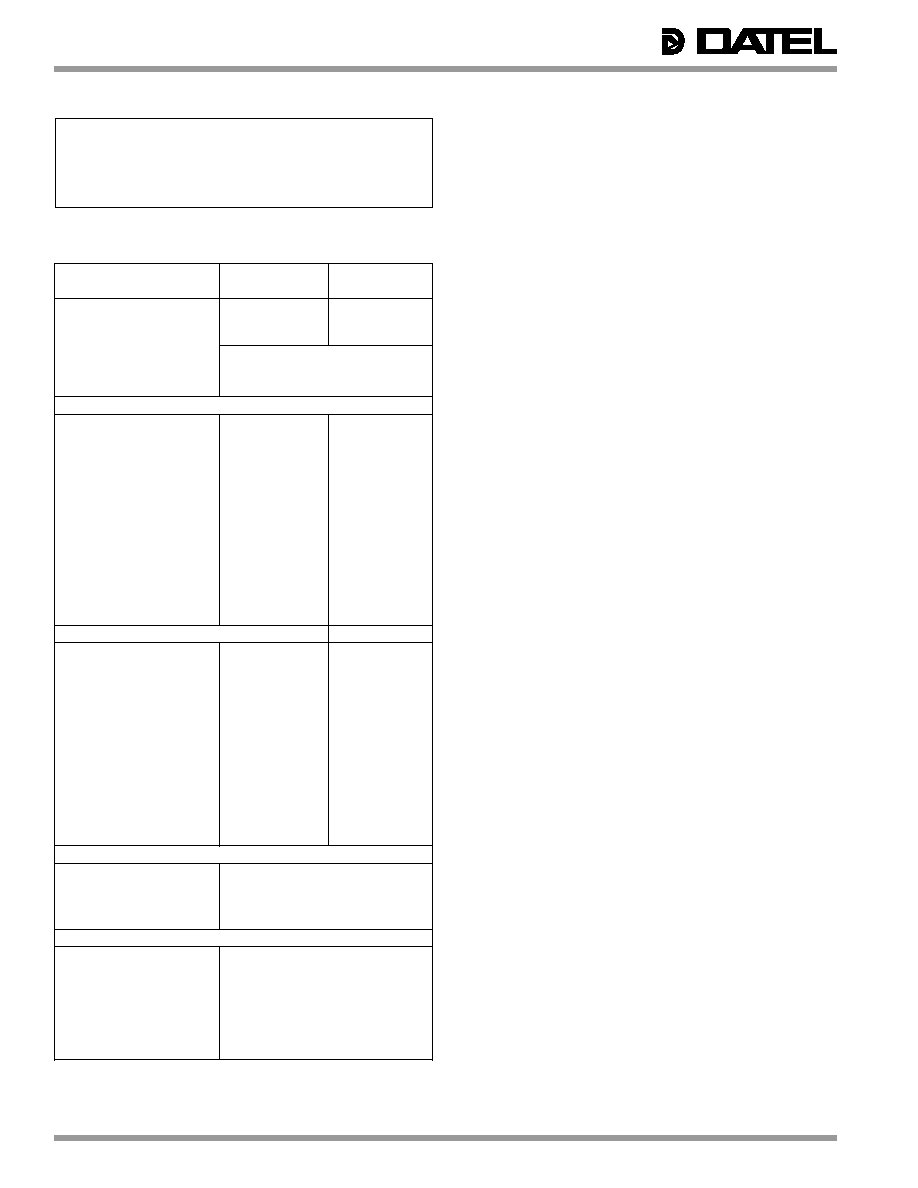
Figure 1. Functional Block Diagram
FEATURES
∑∑
∑∑
∑
12-Bit binary and 3-digit BCD models
∑∑
∑∑
∑
7 Output ranges
∑∑
∑∑
∑
3Ķs V
OUT
settling time
300ns I
OUT
settling time
∑∑
∑∑
∑
Guaranteed monotonicity over full temperature range
∑∑
∑∑
∑
Integral nonlinearity Ī1/2LSB (binary) and Ī1/4LSB
(BCD), maximum
∑∑
∑∑
∑
Differential nonlinearity Ī3/4LSB (binary) and Ī1/4LSB
(BCD), maximum
∑∑
∑∑
∑
High-reliability QL versions available
PIN
FUNCTION
PIN
FUNCTION
1
BIT 1 (MSB)
24
REFERENCE OUT
2
BIT 2
23
GAIN ADJUST
3
BIT 3
22
+15V SUPPLY
4
BIT 4
21
GROUND
5
BIT 5
20
CURRENT OUTPUT
6
BIT 6
19
20V RANGE
7
BIT 7
18
10V RANGE
8
BIT 8
17
BIPOLAR OFFSET
9
BIT 9
16
REFERENCE IN
10
BIT 10
15
VOLTAGE OUTPUT
11
BIT 11
14
≠15V SUPPLY
12
BIT 12 (LSB)
13
NO CONNECTION
INPUT/OUTPUT CONNECTIONS
GENERAL DESCRIPTION
The DAC-HZ Series are high-performance, monolithic, 12-bit
binary and 3-digit BCD, digital-to-analog converters. The
DAC-HZ Series are complete and self-contained with a
precision internal reference and fast output operational
amplifier. Pin programmable output voltage and current
ranges are provided for a high degree of application flexibility;
the binary versions offer 5 output voltage ranges and two
current ranges while the BCD models offer 3 and 1 output
ranges, respectively.
The DAC-HZ Series contains a precision embedded Zener
reference circuit. This eliminates code-dependent ground
currents by routing current from the positive supply to the
internal ground node as determined by the R-2R ladder
network. The internal feedback resistors for the on-board
amplifier track the ladder network resistors, enhancing
temperature performance. The excellent tracking of the
resistors results in temperature coefficients for differential
nonlinearity, zero and gain of Ī2, Ī3 and Ī20ppm/įC
maximum, respectively.
MSB
BITS BCD
BITS BINARY
6.3k
W
LSB
1 2 3 4
REFERENCE OUT 24
GAIN ADJUST 23
BIPOLAR OFFSET
18
+15V
SUPPLY
22
20
19
17
21
5 6 7 8 9 10 11 12
D/A CONVERTER
GROUND
20V RANGE
≠15V
SUPPLY
+6.3V
REFERENCE
1 2 3 4 5 6 7 8 9 10 11 12
1
2
4
8
10
20
40
80
10
0
2
00
4
00
80
0
5k
W
5k
W
(4k
W
, BCD)
15
16
REFERENCE IN
10V RANGE
CURRENT OUTPUT
VOLTAGE OUTPUT
NO INTERNAL
CONNECTION
14
13
*
*
FOR BCD MODELS,
THIS RESISTOR IS
OPEN CIRCUIT.
(4k
W
, BCD)

DAC-HZ Series
ģ
ģ
DAC-HZ12B
DAC-HZ12D
INPUTS
(BINARY)
(BCD)
Resolution
12 binary bits
3 BCD digits
Coding, Unipolar Output
Comp. binary
Comp. BCD
Coding, Bipolar Output
Comp. off. binary
--
Input Logic Level, Bit ON ("0")
0V to +0.8V at ≠1mA
Input Logic Level, Bit OFF ("1")
+2.4V to +5.5V at +40
Ķ
A
Logic Loading
1 TTL load
PERFORMANCE
Voltage Output Nonlinearity
Ī1/2LSB max.
Ī1/4LSB max.
Differential Nonlinearity
Ī3/4LSB max
Ī1/4LSB max.
Gain Error, Before Trimming
Ī0.1%
Zero Error, Before Trimming
Ī0.1% of FSR
Gain Tempco, maximum
Ī20ppm/įC
Zero Tempco, Unipolar, max.
Ī3ppm/įC of FSR
Offset Tempco, Bipolar, max.
Ī10ppm/įC of FSR
Diff. Nonlinearity Tempco, max.
Ī2ppm/įC of FSR
Monotonicity
Over oper. temp. range
Settling Time, I
OUT
to Ī1/2LSB
300ns
Settling Time, V
OUT
to Ī1/2LSB
3
Ķ
s
Slew Rate
Ī10V/
Ķ
s
Power Supply Rejection
Ī0.006%FSR/%Sup.
OUTPUTS
Output Current, Unipolar
0 to ≠2mA, Ī20%
0 to ≠1.25mA, Ī10%
Output Current, Bipolar
Ī1mA, Ī20%
--
Compliance Voltage, I
OUT
Ī2.5V
Output Impedance, I
OUT
, Unipolar
2k
Output Impedance, I
OUT
, Bipolar
2k
--
Output Voltage Ranges, Unipolar
0 to +5V
0 to +2.5V
0 to +10V
0 to +5V
0 to +10V
Output Voltage Ranges, Bipolar
Ī2.5V
--
Ī5V
--
Ī10V
--
Output Current, V
OUT
Ī5mA min.
Output Impedance, V
OUT
0.05
POWER REQUIREMENTS
Power Supply Voltages
+15V, Ī0.5V at 16mA
≠15V, Ī0.5V at 20mA
Ī12V operation
Power Dissipation, maximum
500mW
PHYSICAL ENVIRONMENTAL
Operating Temp. Ranges, Case
0įC to +70į and ≠55įC to +125įC
Storage Temp. Range
≠65įC to +150įC
Thermal Impedance
jc
7.4įC/W
ca
36.6įC/W
Package Type
24-pin DDIP
Weight
0.22 ounces (6.3 grams)
ABSOLUTE MAXIMUM RATINGS
Positive Supply, Pin 22
+18V
Negative Supply, Pin 14
≠18V
Digital Input Voltage, Pins 1≠12
+5.5V
Output Current, Pin 15
Ī20mA
Lead Temperature (soldering, 10s)
300įC
FUNCTIONAL SPECIFICATIONS
(Typical at +25įC and Ī15V supplies unless otherwise noted.)
* Specifications same as first column.
-- No equivalent specifications
Footnotes
FSR is full-scale range and is 10V for 0 to +10V or ≠5V to +5V outputs, 20V for
Ī10V output, etc.
Initial gain and offset errors are trimmable to zero. See Connection Diagrams.
Current output mode.
For 2.5k
or 5k
feedback. For 10k
feedback, the settling time is 4Ķs.
For Ī12V operation of binary models, contact factory.
TECHNICAL NOTES
1. The DAC-HZ12 Series converters are designed and factory
calibrated to give Ī1/2LSB linearity (binary version) and
Ī1/4LSB linearity (BCD version) with respect to a straight
line between end points. This means that if zero and full
scale are exactly adjusted externally, the relative accuracy
will be Ī1/2LSB (Ī1/4LSB, BCD version) everywhere over
the full output range without any additional adjustments.
2. These converters must be operated with local supply by-
pass capacitors from +15V to ground and ≠15V to ground.
Tantalum type capacitors of 1ĶF are recommended and
should be mounted as close as possible to the converter.
If the converters are used in a high-frequency noise
environment, a 0.01ĶF ceramic capacitor should be used
across each tantalum capacitor.
3. When operating in the current output mode, the equivalent
internal current source of 2mA (1.25mA, BCD) must drive
both the internal source resistances and the external load
resistor. A 300ns output settling time is achieved for the
voltage across a 100
load resistor; for higher value
resistors the settling time becomes longer due to the output
capacitance of the converter. For fastest possible voltage
output for a large transition, an external fast-settling
amplifier such as DATEL's AM-500 should be used in the
inverting mode. Settling time of less than 1Ķs can be
achieved. See application diagram.
CALIBRATION PROCEDURE
1. Select the desired output range and connect the converter
as shown in the Output Range Selection tables and the
connection diagrams.
2. To calibrate, refer to the coding tables. Note that
complementary coding is used.
3. Zero and Offset Adjustments
For unipolar operation set all digital inputs to "1" (+2.0 to
+5.5V) and adjust the ZERO ADJUST potentiometer for
zero output voltage or current. For bipolar operation set all
digital inputs to "1" and adjust the OFFSET ADJUST
potentiometer for the negative full scale (for voltage out) or
positive full scale (for current out) output value shown in the
coding table.
4. Gain Adjustment
Set all digital inputs to "0" (0V to +0.8V) and adjust the
GAIN ADJUST potentiometer for the positive full scale (for
voltage out) or negative full scale (for current out) output
value shown in the coding table.

DAC-HZ Series
ģ
ģ
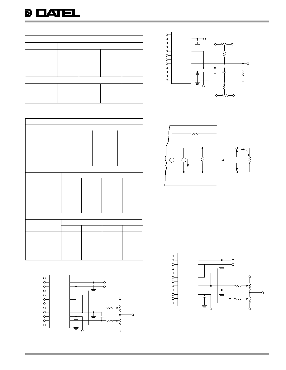
DAC-HZ12B Binary Output Range Selection
OUTPUT RANGE SELECTION TABLES
V
OUT
RANGE
CONNECT THESE PINS TOGETHER
Figure 2. Unipolar Voltage Output Connections
Ī10V
15 & 19
17 & 20
--
16 & 24
Ī5V
15 & 18
17 & 20
--
16 & 24
Ī2.5V
15 & 18
17 & 20
19 & 20
16 & 24
+10V
15 & 18
17 & 21
--
16 & 24
+5V
15 & 18
17 & 21
19 & 20
16 & 24
Ī1mA
--
17 & 20
--
16 & 24
DAC-HZ12D BCD Output Range Selection
+10V
15 & 19
17 & 21
--
16 & 24
+5V
15 & 18
17 & 21
--
16 & 24
+2.5V
15 & 18
17 & 21
19 & 20
16 & 24
≠1.25mA
--
17 & 21
--
16 & 24
BINARY INPUT CODE
Unipolar Output, Complementary Binary
0000
0000 0000
+9.9976V
+4.9988V
≠1.9995
0011
1111
1111
+7.5000
+3.7500
≠1.5000
0111
1111
1111
+5.0000
+2.5000
≠1.0000
1011
1111
1111
+2.5000
+1.2500
≠0.5000
1111
1111
1110
+0.0024
+0.0012
≠0.0005
1111
1111
1111
0.0000
0.0000
0.0000
BCD INPUT CODE
Unipolar Output, Complementary BCD
MSB
LSB
0 to +10V
0 to +5V
0 to +2.5V 0 to ≠2mA
UNIPOLAR OUTPUT RANGES
MSB
LSB
0 to +10V
0 to +5V
0 to ≠2mA
UNIPOLAR OUTPUT RANGES
0110
0110
0110
+9.990
+4.995
+2.498
≠1.2488
1000
1010
1111
+7.500
+3.750
+1.875
≠0.9375
1010
1111
1111
+5.000
+2.5000
+1.250
≠0.6250
1101
1010
1111
+2.5000
+1.250
+0.625
≠0.3125
1111
1111
1110
+0.0100
+0.005
+0.003
≠0.0013
1111
1111
1111
0.0000
0.0000
0.0000
0.0000
BIPOLAR OUTPUT RANGES
INPUT CODE
Bipolar Output, Complementary Offset Binary
MSB
LSB
Ī10V
Ī5V
Ī2.5V
Ī1mA
0000
0000 0000
+9.9951
+4.9976
+2.4988
≠0.9995
0011
1111
1111
+5.0000
+2.5000
+1.2500
≠0.5000
0111
1111
1111
0.0000
0.0000
0.0000
0.0000
1011
1111
1111
≠5.0000
≠2.5000
≠1.2500
+0.5000
1111
1111
1110
≠9.9951
≠4.9976
≠2.4988
+0.9995
1111
1111
1111
≠10.0000
≠5.0000
≠2.5000
+1.0000
OUTPUT CODING TABLES
CONNECTION DIAGRAMS
13
14
15
16
17
18
19
20
21
22
23
24
+15V
12
11
10
9
8
7
6
5
4
3
2
1
1ĶF
1ĶF
= 0 TO +10V
V
≠15V
C (0.001
TO 0.01ĶF)
2.8M
BIT
12
11
10
9
8
7
6
5
4
3
2
1
LSB
MSB
DIGITAL
INPUTS
2.2M
OUT
+15V
≠15V
GAIN ADJUST
10k
TO 100k
ZERO ADJUST
10k
TO 100k
+15V
DAC-HZ12B
or DAC-HZ12D
(BOTTOM VIEW)
Voltage output is at pin 15; current output is at pin 20.
Figure 3. Unipolar Current Output Connections
13
14
15
16
17
18
19
20
21
22
23
24
+15V
12
11
10
9
8
7
6
5
4
3
2
1
1ĶF
1ĶF
= 0 TO ≠200mV
V
≠15V
C (0.001
TO 0.01ĶF)
2.8M
BIT
12
11
10
9
8
7
6
5
4
3
2
1
LSB
MSB
DIGITAL
INPUTS
2.2M
OUT
GAIN ADJUST
10k
TO 100k
ZERO ADJUST
10k
TO 100k
+15V
DAC-HZ12B
or DAC-HZ12D
(BOTTOM VIEW)
≠15V
≠15V
100
+15V
I
OUT
= 0 TO ≠2mA
BIPOLAR OFFSET
CURRENT OUT
R
EQ
= R
O
= 5k for unipolar operation
R
EQ
= R
R
= 2.8k for bipolar operation
I
OUT
= 2mA binary
= 1.25mA BCD
*This resistor is open circuit for BCD models
6.3V
+
≠
DAC-HZ12B or DAC-HZ12D
I
OUT
R
O
R
EQ
I
L
R
L
R
R
= Ī2.5V Maximum
(Output compliance voltage)
V
OUT
V
OUT
17
20
21
5k
6.3k
*
GND
|| R
O
Figure 4. Equivalent Current Mode Output Circuit
13
14
15
16
17
18
19
20
21
22
23
24
+15V
12
11
10
9
8
7
6
5
4
3
2
1
1ĶF
1ĶF
= ≠5 TO +5V
V
≠15V
C (0.001
TO 0.01ĶF)
2.8M
BIT
12
11
10
9
8
7
6
5
4
3
2
1
LSB
MSB
DIGITAL
INPUTS
2.2M
OUT
+15V
≠15V
GAIN ADJUST
10k
TO 100k
ZERO ADJUST
10k
TO 100k
+15V
DAC-HZ12B
(BOTTOM VIEW)
Figure 5. Bipolar Voltage Output Connections

DAC-HZ Series
ģ
ģ
Figure 6. Bipolar Current Output Connections
ģ
ģ
DATEL makes no representation that the use of its products in the circuits described herein, or the use of other technical information contained herein, will not infringe upon existing or future patent rights. The descriptions contained herein
do not imply the granting of licenses to make, use, or sell equipment constructed in accordance therewith. Specifications are subject to change without notice. The DATEL logo is a registered DATEL, Inc. trademark.
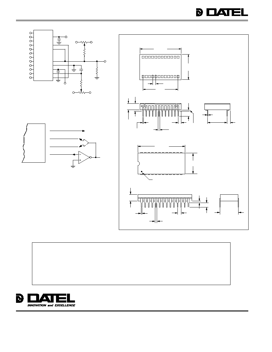
MECHANICAL DIMENSIONS INCHES (mm)
Figure 7. Using a High-Speed External Op Amp for
Faster Settling
13
14
15
16
17
18
19
20
21
22
23
24
+15V
12
11
10
9
8
7
6
5
4
3
2
1
1ĶF
1ĶF
Ī100mV
V
≠15V
C (0.001
TO 0.01ĶF)
2.8M
BIT
12
11
10
9
8
7
6
5
4
3
2
1
LSB
MSB
DIGITAL
INPUTS
2.2M
OUT
GAIN ADJUST
10k TO 100k
ZERO ADJUST
10k
TO 100k
+15V
DAC-HZ12B
(BOTTOM VIEW)
≠15V
≠15V
100
+15V
I
OUT
= Ī1mA
BIPOLAR OFFSET
17
10V RANGE
Pin 20 or 21
18
20V RANGE
19
CURRENT OUT
20
DAC-HZ12B
or
DAC-HZ12D
X
A
External high-speed inverting op amp; use DATEL's AM-500
for less than 1Ķsec output settling.
A =
Refer to the output range selection tables, Tables 1 and 2.
Wherever pin 15 appears, use pin X of the external amplifier and
scale as desired.
0.500/0.610
(12.70/15.49)
DATEL
PIN 1
IDENTIFIER
1
24
0.225 MAX.
(5.72 MAX.)
0.030 / 0.070
(0.76 / 1.78)
0.014 / 0.023
(0.36/0.58)
0.100 TYP.
(2.54)
0.590/0.620
(14.98/15.74)
1.290 MAX.
(32.77 MAX.)
0.120 / 0.200
(3.05 / 5.08)
0.015 / 0.075
(0.38 / 1.91)
12
13
0.200 MAX.
(5.080)
0.235 MAX.
(5.969)
0.600 Ī0.010
(15.240)
0.80 MAX.
(20.32)
0.100 TYP.
(2.540)
0.100
(2.540)
0.018 Ī0.002
(0.457)
0.100
(2.540)
0.040
(1.016)
1.31 MAX.
(33.27)
1
12
13
24
1.100
(27.940)
0.190 MAX.
(4.826)
0.010
(0.254)
+0.002
≠0.001
SEATING
PLANE
0.025
(0.635)
Dimension Tolerances
(unless otherwise indicated):
2 place decimal (.XX) Ī0.010 (Ī0.254)
3 place decimal (.XXX) Ī0.005 (Ī0.127)
Lead Material:
Kovar alloy
Lead Finish:
50 microinches (minimum)
gold plating over 100 microinches
(nominal) nickel plating
OPERATING
OUTPUT
MODEL
TEMP. RANGE
CODING
DAC-HZ12BGC
0 to +70įC
Binary
DAC-HZ12BMC
0 to +70įC
Binary
DAC-HZ12BMM
≠55 to +125įC
Binary
DAC-HZ12BMM-QL
≠55 to +125įC
Binary
OPERATING
OUTPUT
MODEL
TEMP. RANGE
CODING
DAC-HZ12DGC
0 to +70įC
BCD
DAC-HZ12DMC
0 to +70įC
BCD
DAC-HZ12DMM
≠55 to +125įC
BCD
DAC-HZ12DMM-QL
≠55 to +125įC
BCD
Contact DATEL for information concerning our QL high-reliability screening program.
ORDERING INFORMATION
DATEL, Inc. 11 Cabot Boulevard, Mansfield, MA 02048-1151
Tel: (508) 339-3000
(800) 233-2765 Fax: (508) 339-6356
Internet: www.datel.com Email: sales@datel.com
DATEL (UK) LTD. Tadley, England Tel: (01256)-880444
DATEL S.A.R.L. Montigny Le Bretonneux, France Tel: 01-34-60-01-01
DATEL GmbH MŁnchen, Germany Tel: 89-544334-0
DATEL KK Tokyo, Japan Tel: 3-3779-1031, Osaka Tel: 6-6354-2025
DS-0134 1996

