 | –≠–ª–µ–∫—Ç—Ä–æ–Ω–Ω—ã–π –∫–æ–º–ø–æ–Ω–µ–Ω—Ç: DVME-613A | –°–∫–∞—á–∞—Ç—å:  PDF PDF  ZIP ZIP |

DVME-613
Isolated Industrial 16S or 8D
Channel VME A/D Board
PRODUCT DATA
Æ
Æ
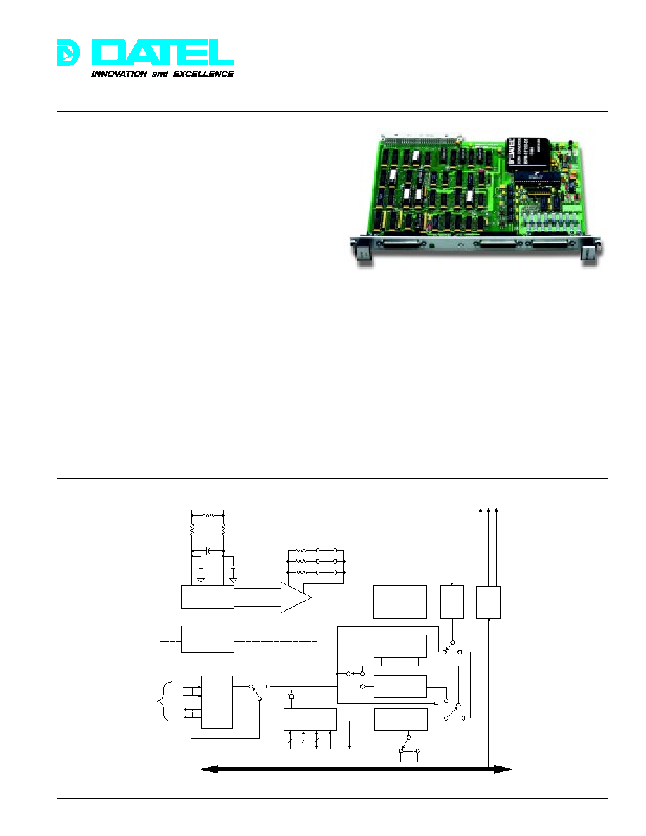
Figure 1. DVME-613 Simplified Block Diagram
FEATURES
∑∑
∑∑
∑
16 single-ended or 8 differential analog input channels
∑∑
∑∑
∑
12, 14, or 16-bit A/D resolution
∑∑
∑∑
∑
Isolation to ±500V
∑∑
∑∑
∑
On-board programmable gain amplifier and start timer
∑∑
∑∑
∑
8 in and 8 out discrete digital lines
∑∑
∑∑
∑
Programmable vectored VME interrupt
∑∑
∑∑
∑
Simple programming for any operating system or
language
Designed for industrail data acquisition, process control, and
factory automation, the DVME-613 is a low-cost isolated
analog input board for VME bus computers. The DVME-613
will accept sixteen single-ended or eight differential input
channels which are all isolated from the VME bus by ±500
Volts. In addition, each channel is protected from adjacent
channel overloads up to ±150 Volts. The common mode
voltage range is ±11 Volts relative to isolated analog ground.
The analog input range is selectable as ±10 Volts for bipolar
inputs or 0 to +10 Volts unipolar. By using an on-board
programmable gain amplifier (PGA), inputs may be accepted
directly from bridges, load cells, RTD's, and strain gauges.
The PGA includes selectable gain ranges of times one, ten,
and on hundred for low level inputs.
An optional signal conditioning pad area accepts shunt
resistors, attenuators, hash filters, and clamps. This allows
direct input from isolated 1-5 mA or 4-20 mA transmitters and
from voltage sources greater than ±10 Volts full scale. For
bridge-type sensors, on-board regulated DC excitation voltage
is provided which is fully isolated from VME bus.
The DVME-613 inputs are plug compatible with DATEL's
DVME-691 rack-mount signal conditioning panel for screw
terminal inputs. Three A/D converter options are offered. The
DVME-613A is a 12-bit A/D converter with overall accuracy of
±0.05% of full scale. Resolution of the DVME-613A is 2.5
millivolts per count for unipolar inputs.
The DVME-613B offers a 14-bit A/D converter and for highest
resolution inputs, a 16-bit converter is included on the DVME-
613C. All models produce left-justified data outputs so that
boards may be interchanged without having to rewrite existing
software to scale the data. A/D conversion takes 24
microseconds for the DVME-613A. The sampling A/D
converter design offers continuous automatic recalibraion. To
insure reliability in industrial process control environments,
lcoal channels may be dedicated to ground and reference
inputs for self-testing of signal paths.
V M E b u s P 1
D i g i t a l
I / O
P o r t s
8 T T L
I n
8 T T L
O u t
J 3
N o n - i s o l . t r i g / l a t c h
L a t c h
V M E b u s
I n t e r f a c e
A M x
A 2 3
- A 1
D 1 5
- D 0
S Y S
C L K
D T A C K *
L E D
L a m p
I R Q *
1 - 7
V M E I n t e r r u p t
R e q u e s t
S t a r t T i m e r
A / D L o g i c ,
C o m m a n d /
S t a t u s R e g i s t e r
S t a r t
E O C
S a m p l i n g
A / D C o n v e r t e r
D C / D C
C o n v .
+ 5 V d c
J 2
I s o l a t e d
D C P o w e r
J 1
E x t e r n a l
T r i g g e r
I n p u t
( I s o l a t e d )
I s o l a t i o n B a r r i e r
P r o g r a m m a b l e
G a i n
A m p l i f i e r
A n a l o g
M u l t i p l e x e r
J 1
1 6 S E / 8 D
A n a l o g C h a n n e l I n p u t s
O n - b o a r d s i g n a l
c o n d i t i o n i n g p a d
a r e a f o r s h u n t s ,
a t t e n u a t o r s , o v e r l o a d
c l a m p s , e t c .
O p t o -
I s o l a t i o n
G a i n S e l e c t i o n
C h a n n e l
A d d r e s s
R e g i s t e r
DATEL, Inc., Mansfield, MA 02048 (USA)
∑
Tel: (508)339-3000, (800)233-2765 Fax: (508)339-6356
∑
Email: sales@datel.com
∑
Internet: www.datel.com
161

DVME-613
Æ
Æ
DATEL, Inc., Mansfield, MA 02048 (USA)
∑
Tel: (508)339-3000, (800)233-2765 Fax: (508)339-6356
∑
Email: sales@datel.com
∑
Internet: www.datel.com
PGA Settling Delay
10 µs, gain = 1 (after
channel selection)20 µs,
gain = 10; 100 µs, gain =
100
A/D Output Resolution
12 bits (DVME-613A)
14 bits (DVME-613B)
16 bits (DVME-613C)
A/D Output Coding
Selectable as unipolar
straight binary or bipolar
offset binary
Accuracy at +25∞C
(After recalibration)
(Gain = 1 or 10)
613A: ±0.05% of FSR
(Gain = 100)
613A: ±0.1% of FSR
(Gain = 1)
613B: ±0.0125% of FSR
(Gain = 1)
613C: ±0.0075% of FSR
Nonlinearity
±0.5 LSB
Temp. Coefficient of Zero
±20 ppm/∞C of FSR
Temp. Coefficient of Gain
±20 ppm/∞C of FSR
A/D Conversion Period
613A: 24 µs*
613B: 28 µs*
613C: 32 µs*
A/D Converter Start Sources
External isolated TTL
trigger, local pacer start
clock, VME command write,
or VME A/D data read. The
TTL trigger occurs on the
rising edge. Trigger width
0.1 to 5 µs.
Monotonicity
No missing codes
A/D Start Clock
May be jumpered to start
an A/D conversion/VME
bus interrupt
Start Clock Range
32 µs to 5 minutes,
jumperable in x2 steps.
Derived from 16 MHz VME
bus SYSCLK.
Discrete I/O Lines
8 inputs and 8 outputs,
non-isolated, latch control
for inputs
Discrete I/O TTL Levels
Inputs: "0" <0.8V, "1"> 2.0V
Outputs: "0" <0.4V, "1"> 2.4V
Discrete TTL I/O Loading
1 TTL-LS load plus 4.7 K
pullup to +5V output.
Output: 24 mA
LED Lamp
Front panel lamp software
controlled by register bit.
May be used for power up
test, alarms, etc. Defaults
to dark at power up or bus
reset.
ANALOG INPUTS
Number of Channels
16SE or 8 diff. channels
Full Scale Input Ranges
Unipolar
Bipolar
Gain = 1
0 to 10V
±10V
Gain = 10
0 to 1V
±1V
Gain = 100
0 to 100 mV
±100 mV
Input Isolation
±500V max. from analog
section to VME bus
Isolation Capacitive Coupling
25 pF analog section to VME
Isolation Resistive Coupling
100 M
analog to VME
Common Mode Voltage Range
±11V to isolated ground
Common Mode Rejection
86 dB, dc to 60 Hz, gain =
100, 1 K
source unbalance
Channel-to-Channel Protection
±150V max. sustained
Input Bias Current
±200 picoamps
Input Impedance (power on)
100 M
to isolated ground
Input Impedance (power off)
33 K
to isolated ground
Programmable Gain Amplifier
Jumper selectable for gains
of 1, 10, or 100. Will accept
precision resistor for user
defined gain.
FUNCTIONAL SPECIFICATIONS
(Typical at +25∞C, gain = 1, unless otherwise noted)
DIGITAL SECTION
A/D conversion may be started from several sources including
an external isolated trigger input, the local start timer, a
memory write from the host or a read of the A/D data register.
The maskable vectored VME bus interrupt may originate from
an external trigger, the local timer or the A/D EOC data ready
signal.
VME bus interrupts are fully vectored using selectable IRQ 1-
7 levels.
The A/D data ready EOC signal is indicated in a status
register and maskable VME bus interrupt. All modes are
software controlled by local command and status registers.
The DVME-613 provides 16 digital lines for logic control of
devices such as pumps, heaters, and valves. These lines are
TTL logic compatible and arranged as eight inputs and eight
outputs. A separate control input latches the eight TTL input
lines.
The DVME-613 is a VME bus SA24:SD16 slave. The board
appears to the VME bus as a memory-mapped 8-word
contiguous block of 16-bit registers using 24-bit addressing
and six address modifiers. All types of 16- and 32-bit host
CPU's may control the board on 16-bit word access using any
software language.
The VME bus interface uses only the P1 backplane connector
for compatibility with most hosts. All analog and digital port
interfacing uses front panel connectors to avoid conflict with
P2 bus connector usage. A front panel LED lamp may be
programmed by host software for board power-up test or for
alarms.
Operating temperature range of the DVME-613 is 0 to +60∞C.
The board measures 9.19" x 6.3" x 0.6", using the standard
6U VME bus outline. All power is supplied by VME bus
requiring +5 Volts DC at 2.5 Amps.
The board includes a free software program disk and a
comprehensive user's manual. The source-code software is
heavily commented and may be easily adapted for any
operating system or host language. Application engineering
consultation is available to users.
162

DVME-613
Æ
Æ
DATEL, Inc., Mansfield, MA 02048 (USA)
∑
Tel: (508)339-3000, (800)233-2765 Fax: (508)339-6356
∑
Email: sales@datel.com
∑
Internet: www.datel.com
VME BUS INTERFACE
Standards of Compliance
IEEE P1014/D1.0
Architecture
SAD24:SD16 slave
consisting of 8 continguous
word registers
Data Bus Width
16 bits using P1 connector
Address Bus
24 address lines (A23-A1)
plus 6 Address Modifiers
Address Modifier Codes
39 or 3D hex, selectable
VME bus Interrupt
1 line, selectable IRQ 1-7*.
Asserts maskable
programmable 8-bit vector
ID code.
Interrupt Source
Selectable from external
trigger, start timer, or A/D
data ready.
Data Transfer
Uses 16 MHz VME bus
SYSCLK signal to generate
DTACK* signal with
selectable delay.
VME bus, P1
96-pin male DIN connector.
The P2 connector is not
used.
Local Isolated Analog Intput
J1 connector, 25-pin
and Isolated Trigger
DB-25S female on front
panel, pin-compatible to
DVME-691 screw terminator.
Isolated DC Power
J2 connector, 25-pin
DB-25S female on front
panel. Power available:
±15V dc at 25 mA max.
Discrete Digital I/O
J3 connector, 25-pin DB-25S
female on front panel
TYPICAL BRIDGE-TYPE INPUT CONNECTIONS
Figure 2 shows the DVME-613 connected to a bridge-type
transducer. Notice that the bridge excitation is derived from
the +15V dc power available from the DVME-613. The
excitation voltage is regulated but not extremely high-
precision.
To compensate for this, use a precision voltage divider and
measure the excitation supply using a spare differential
channel. Then use this value to do a software autocalibration
with each channel scan.
CONNECTORS
MISCELLANEOUS
Power Required
+5V dc, ±5% at 2.5A max.
from VME bus
Operating Temp. Range
0 to +60 ∞C
Storage Temp. Range
≠20 to +80 ∞C
Relative Humidity
10% to 90%, non-condensing
Altitude
0 to 10,000 feet
Outline Dimensions
Double height VME,
6U outline.
9.19"W x 6.3"D x 0.6"H
(233,5 x 160 x 15,24 mm)
Weight
17 oz. (482 grams)
*Single channel conversion rates are shown. For mutlichanenl
inputs, an additional 20 µs must be allowed after channel
selection before the next A/D conversion start.
Figure 2. Typical Bridge-type Input Connections
I s o l a t e d + 1 5 V d c E x c i t a t i o n
C h a n . 0 H i I n
C h a n . 0 L o I n
I s o l a t e d P o w e r G r o u n d
J 1 - 2 4
J 2 - 1 4
J 1 - 1 2
J 2 - 1 5
S e n s o r o r T r a n s d u c e r
B r i d g e
D V M E - 6 1 3
I s o l a t i o n B a r r i e r
V M E B u s
163

DVME-613
Æ
Æ
DATEL, Inc., Mansfield, MA 02048 (USA)
∑
Tel: (508)339-3000, (800)233-2765 Fax: (508)339-6356
∑
Email: sales@datel.com
∑
Internet: www.datel.com
REGISTER PROGRAMMING
Register Memory Mapping
BASE address switches must be selected for even address
boundaries. All registers must be accessed on 16-bit word
memory operations.
Address
Direction
Description
(hex)
BASE + 0
Write
Command register
BASE + 0
Read
Status register
BASE + 2
Write
Channel address register
BASE + 4
Write
Start A/D conversion register
BASE + 6
Read
A/D data register
BASE + 8
Write
Interrupt vector ID register
BASE + 8
Read
Interrupt vector ID register
BASE + A
Write
Calibrate A/D converter
BASE + C
Write
TTL digital output port register
BASE + E
Read
TTL digital inut port register
Command/Status Register (Write/Read BASE + 0)
15
8
7
6
5
4
3
2
1 0
EOC
OVR
INT LED
X
X
X
CNV
Start Mode
SMP ENB ON
ENB
("x" bits are don't care or not defined)
If interrupt is not used, the host should poll EOC before
reading A/D data. Teh read of the A/D data register resets
EOC to 0 even if anotehr conversion is not started.
End of Conversion
0 = Conversion in progress. Data not
EOC [Bit 15]
valid.
1 = Conversion done. Data ready.
Over Sample Error
0 = No error
OVR SMP [Bit 8]
1 = Oversampling error (conversion
(read only)
start while EOC = 0, A/D busy)
VME Interrupt Enabled 0 = Interrupt disabled
INT ENB [Bit 7] R/W
1 = Interrupt enabled (interrupts may
be jumpered from A/D EOC,
external trigger or internal timer)
Front Panel Lamp
0 = LED lamp off
LED [Bit 6] R/W
1 = LED lamp on
A/D Conversion Enabled 0 = Disable A/D conversions
CNV ENB [Bit 2] R/W 1 = Enable A/D conversions
A/D Start Mode
Source of A/D start:
[Bits 1, 0] R/W
00 = Host write to BASE + 4
01 = Read A/D data register
10 = Internal start timer
11 = External TTL trigger
Program the command register last. All registers default to
zeroes at power-up.
Channel Address Register (Write BASE + 2)
15
7
6
5
4
3
2
1
0
X
GP1
GP0
X
X
Chn
Chn Chn
Chn
Adr
Adr
Adr
Adr
3
2
1
0
GP1, GP0 (bits 7, 6) - These are spare unassigned register
output bits available for any purpose. They appear at
integrated circuit U19-10, 12.
Chn Adr (bits 3-0) - Channel Address input corresponds to
A/D channels 0 through 7 (differential) or 0 through 15 (single-
ended).
Start A/D Conversion Register (Write BASE + 4)
15
7
6
5
4
3
2
1
0
X
X
X
X
X
X
X
X
X
An A/D conversion may be started by a write to this register if
enabled by the command register mode 00. EOC willb e set
to 0 after conversion is started and until data is ready.
A/D Data Register (Read BASE + 6)
15
7
6
5
4
3
2
1
0
MSB
LSB
LSB
LSB
ALL
12
14
16
A/D data is left justified for all converters. The least significant
bit for the 12-bit DVME-613A is bit 4 with bits 3-0 filled with
zeroes. The LSB for the 14-bit DVME-613B is bit 2 with zero
vill. For the 16-bit DVME-613C, the LSB is bit 0.
For bipolar converters, the MSB is used as a polarity bit and is
set to offset binary (1 = positive).
VME bus Interrupt ID Register (Read/Write BASE + 8)
15
7
6
5
4
3
2
1
0
X
V07
V06
V05
V04
V03
V02
V01
V00
An 8-bit interrupt ID code is used. Before writing the ID code
from the host, this register may be sued for board testing. A
valid power-up test would be to write then readback and
confirm a range of values to this register before enabling
interrupts. Portions of the command/status register may also
be used for write/readback tests. Such tests would confirm
the bus interface and register logic. Furhter testing may be
done using the dedicated reference inputs to the A/D
converter. If all tests succeed, the front panel LED lamp may
be lit.
164

DVME-613
Æ
Æ
DATEL, Inc., Mansfield, MA 02048 (USA)
∑
Tel: (508)339-3000, (800)233-2765 Fax: (508)339-6356
∑
Email: sales@datel.com
∑
Internet: www.datel.com
Calibrate A/D Converter (Write BASE + A)
15
7
6
5
4
3
2
1
0
X
X
X
X
X
X
X
X
X
Writing to this register will start an A/D calibration cycle for
approximately 320 milliseconds until EOC. This operation
should be done once after power up. During calibration, the
A/D converter makes internal corretins. Periodic calibration is
optional in stable temperature environments but is suggested
frequently with changing temperatures.
Discrete Digital Output Register (Write BASE + C)
15
7
6
5
4
3
2
1
0
X
D07
D06 D05 D04 D03 D02 D01 D00
Discrete Digital Input Register (Read BASE + E)
15
7
6
5
4
3
2
1
0
X
V07
V06
V05
V04
V03
V02
V01
V00
FRONT PANEL INPUT/OUTPUT CONNECTIONS
Pin numbering is shown as viewed from the front panel
Discrete Non-isolated Digital I/O - Connector J3
Isolated DC Power Out - Connector J2
Isolated Analog Inputs - Connector J1
Channel address notation: Single-ended/Differential
Figure 3. Cabling the DVME-613 using DATEL's
DVME-691 Screw Terminator Panel
DVME-691A Screw
Terminator Panel
Signal Screw
Terminals
Signal wiring bundle to/from
sensors and actuators
Host VME
Computer
Signal Conditioning P
ads
19" Rack (not shown)
DVME-613 A/D Board
13
12
11
10
9
8
7
6
5
4
3
2
1
External Trig*/Latch In
Digital Ground
Digital Out 5
Digital Out 4
Digital Ground
Digital Out 1
Digital Out 0
Digital Ground
Digital In 5
Digital In 4
Digital Ground
Digital In 1
Digital In 0
25
24
23
22
21
20
19
18
17
16
15
14
Digital Out 7
Digital Out 6
Digital Ground
Digital Out 3
Digital Out 2
Digital Ground
Digital In 7
Digital In 6
Digital Ground
Digital In 3
Digital In 2
Digital Ground
13
12
11
10
9
8
7
6
5
4
3
2
1
Non-Isol. Digital Ground
+5V dc Out (non-isol.)
No Connection
No Connection
No Connection
Spare to internal pad
Spare to internal pad
Spare to internal pad
Spare to internal pad
No Connection
≠15V dc Out (<25 mA)
Isolated Ground
+15V dc Out (<25 mA)
25
24
23
22
21
20
19
18
17
16
15
14
Non-Isol. Digital Ground
+5V dc Out (non-isol.)
No Connection
No Connection
No Connection
No Connection
No Connection
No Connection
No Connection
≠15V dc Out (<s5 mA)
Isolated Ground
+15V dc Out (<25 mA)
13
12
11
10
9
8
7
6
5
4
3
2
1
Isol. External Trigger In
Chan. 8 Hi/Chan. 0 Lo
Signal Ground
Chan. 1 Hi
Chan. 10 Hi/Chan. 2 Lo
Signal Ground
Chan. 3 Hi
Chan. 12 Hi/Chan. 4 Lo
Signal Ground
Chan. 5 Hi
Chan. 14 Hi/Chan. 6 Lo
Signal Ground
Chan. 7 Hi
25
24
23
22
21
20
19
18
17
16
15
14
Signal Ground
Chan. 0 Hi
Chan. 9 Hi/Chan. 1 Lo
Signal Ground
Chan. 2 Hi
Chan. 11 Hi/Chan. 3 Lo
Signal Ground
Chan. 4 Hi
Chan. 13 Hi/Chan. 5 Lo
Signal Ground
Chan. 6 Hi
Chan. 15 Hi/Chan 7 Lo
165

DVME-613
Æ
Æ
DATEL, Inc., Mansfield, MA 02048 (USA)
∑
Tel: (508)339-3000, (800)233-2765 Fax: (508)339-6356
∑
Email: sales@datel.com
∑
Internet: www.datel.com
ORDERING GUIDE
Model
Description
DVME-613A
12 -bit A/D board
DVME-613A
12 -bit A/D board
DVME-613A
12 -bit A/D board
All models include a comprehensive user's manual and a software disk. All boards are burn-in tested under power-cycled
conditions and include a one-year warranty. DATEL will review custom signal conditioning for quantity requirements.
Accessories
DVME-691A
Screw terminator panel for 19-inch rack mount. Includes flat signal cables to the DVME-613.
PROGRAMMING
The DVME-613 appears to the host computer as a block of
16-bit memory-mapped registers. To program the DVME-613,
read/write emmory word operations may be sued from any
language. In "C", short pointers will access these registers. In
680X0 assembly language, move word (move.w) operations
do the job. Since the DVME-613 is addressed as absolute
memory, any host language or operating system may be
used. In UNIX, a library function may ben needed to map
absolute physical addresses to logical addresses.
Either polled status bits or interrupts may be used to indicate
when A/D data is ready. If you wish to use interrupts, a simple
device driver may be used to send a flag to the Operating
System. A device driver is not necessary for polled operation.
A sample "C" program to control the DVME-613 is listed
below:
/* 613c.c demo 4may89 ldc */
#include <stdio.h>
#include <io.h>
#define SAMPLES 8 /* last channel + 1 to scan */
/* The base address below is set by board switches before
iinstallation. Change this base address for your system */
#define BASPTR 0xFF0000 /* 24-bit address */
/* Make sure all shorts declared below refer to 16-bit words */
unsigned short *base_ptr; /* base address */
/* offsets to board registers: */
unsigned short *ctl_ptr, /* command-status */
*chan_ptr, /* channel address */
*start_ptr, /* start conversion */
*addat_ptr; /* A/D data */
unsigned short outdata[8]; /* array to store A/D samples */
int scan(int samples), channel, wait(int delay);
main( ){
/* initialize pointers to registers.
Note pointer (cast) */
base_ptr = (unsigned short *) BASPTR;
ctl_ptr = (unsigned short *) (BASPTR + 0);
chan_ptr = (unsigned short *) (BASPTR + 2);
addat_ptr = (unsigned short *) (BASPTR + 6);
scan (SAMPLES);
printf("\nA/D data (hex):");
for(channel=0 ; channel < SAMPLES ; channel++ )
printf("\nChan. %d = %x", channel, outdata [channel]);
}/* end of main */
/* Functions
*/
wait(delay){
while(delay--)
;
}
/* Scan( ) collects one scan of A/D samples to outdata[ ] with
sequential channel addressing starting at channel 0. */
scan(samples){
int channel = 0; /* current channel address started at 0 */
/* Initialize command register, no interrupts, LED on,
converter enabled, trigger on A/D data read: */
*ctl_ptr = 0x0045;
*chan_ptr = 0; /* start at channel 0 */
wait(10); /* Adjust this for a 20 microsecond minimum
settling delay whenever the channel address is changed */
/* Do one dummy A/D read to start conversion. This
sample will be overwritten: */
outdata [channel] = *addat_ptr;
while( channel < samples ) {
/* wait for EOC true */
while(( 0x8000 & *ctl_ptr ) != 0x8000 )
;
*chan_ptr = channel + 1; /* bump channel address */
wait(10); /* settling delay */
/* store the last channel and start the next one */
outdata [channel++] = *addat_ptr;
}
}
166
