 | –≠–ª–µ–∫—Ç—Ä–æ–Ω–Ω—ã–π –∫–æ–º–ø–æ–Ω–µ–Ω—Ç: DVME-614L | –°–∫–∞—á–∞—Ç—å:  PDF PDF  ZIP ZIP |

FEATURES
∑∑
∑∑
∑
Up to 10 MHz sample rate
∑∑
∑∑
∑
Choice of 12, 14, or 16-bit A/D resolution
∑∑
∑∑
∑
Very low harmonic distortion
∑∑
∑∑
∑
Optional 2, 4, 8 or 16-channel simultaneous sampling
∑∑
∑∑
∑
On-board FIFO memory for up to 16,384 samples
∑∑
∑∑
∑
Ideal for FFT's, DSP or array-processor "front ends"
∑∑
∑∑
∑
Non-bus burst parallel port for seamless, non-stop
recording
∑∑
∑∑
∑
Analog input comparator trigger
Offering very high system speed, the DVME-614 is a
multichannel analog input board for VMEbus computers.
Maximum input bandwidth is available up to 5 MHz and may
be sampled at up to 10 MHz. A common mother board is
used, with the analog section contained in a pluggable 2" by 4"
module. This allows for a family of several different Sample/
Hold - A/D converter speed and resolution options by
exchanging analog modules.
The analog input ranges of the A/D converters are selectable
as unipolar 0 to +10 V, or bipolar ±5 V or ±10 V depending on
the model. The DVME-614E offers 16 single-ended or 8
differential high speed channels.
The DVME-614F, G, J, K, L, M, N, and P include simultaneous
sample and hold circuitry. This function acquires signals on all
channels at the same time. This protects against phase errors
and negates channel to channel sample time skew.
Applications include high speed cross-channel computation,
beam-former coherency for sonar or acoustics, telemetry,
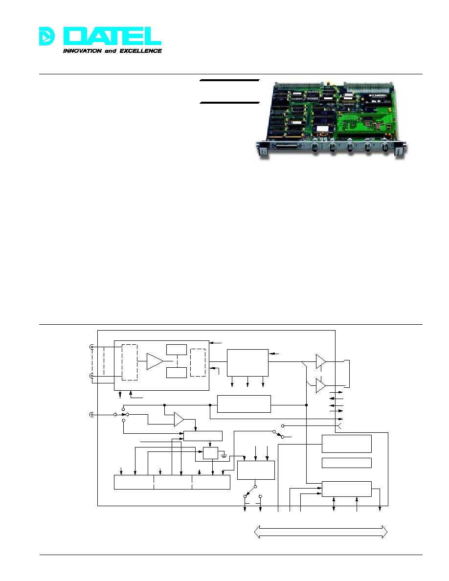
Figure 1. Functional Block Diagram
multiple carrier demodulation, wear testing, vibration analysis,
ultrasound and highly concurrent system testing.
A/D data passes to an on-board First-In, First-Out, (FIFO) data
memory and then to the host computer bus interface under
software control. This design can continuously collect analog
data with non-stop converter triggering while data is
simultaneously read from the FIFO. The FIFO acts to
decouple the precise timing of the A/D section with the block-
oriented data transfers on the bus. This allows for the
collection of "seamless" wide-bandwidth signals of millions of
samples or greater.
Data may be transferred to mass storage peripherals such as
disk or magnetic tape. Applications include long-baseline
studies found in astrophysics, component life testing, and
anomalous pattern search.
The analog section of the DVME-614 series is optimized for high
signal quality and very low dynamic noise. The DVME-614 is
ideal as an FFT "front-end" or DSP quantizer for array processors.
Channel Address Sequencer
FIFO
Memory
Empty Half
Full
Analog
Input
Channels
Trigger Select
Trigger In
D/A Out
External
Trigger
Trigger
Comparator
Analog Trigger
D/A Converter
8MHz
J6 Header
Parallel
Outport
D/A Output
External Clock Input
Ready* Output
Acknowledge* Input
External Enable Input
SSH Control
DC/DC Power
Converter
Registers
VMEbus
Interface
Interrupt
Request
HF
FF
S D
Q
C
Clk Gate Out
Counter 0
Clk
Gate
Out
Counter 2
Clk
Gate
Out
Counter 1
EOC*
Convert Enable
Internal
Trigger
500
kHz
Start Convert
Acq
EOS*
Trig*
82C54 Programmable Interval Timer
IRQ*
1-7
+5V AM
0-5
A23-
A01
D15-
D00
SYSCLK DTACK*
VMEbus P1
J5
FIFO HF/FF*
Sample Counter
Trigger Rate
A/D Start Clock
EOC
Reset
M
U
X
A/D
A/D
Pluggable Analog Section
C
T
L
Start
Convert
DVME-614
High-Speed, Analog Input
Board for VMEbus Computers
Æ
Æ
Up to 16 simultaneous
channels
NEW
DATEL, Inc., Mansfield, MA 02048 (USA)
∑
Tel: (508)339-3000, (800)233-2765 Fax: (508)339-6356
∑
Email: sales@datel.com
∑
Internet: www.datel.com
167

DVME-614
Æ
Æ
DATEL, Inc., Mansfield, MA 02048 (USA)
∑
Tel: (508)339-3000, (800)233-2765 Fax: (508)339-6356
∑
Email: sales@datel.com
∑
Internet: www.datel.com
The A/D conversion timing section is designed for accurate
multi-scan data acquisition. Software programmable timers
control the interval between each conversion and each
multichannel scan. A programmable sample counter allows
sample blocks of specific length independent of FIFO length.
The timer/counter section uses a precision on-board VMEbus
clock or may be replaced by an external timebase. Time-out
and sample count activities may be monitored from the
computer bus using I/O status registers and/or programmable
interrupts.
S/H-A/D triggering may use several sources under software
control. The internal timebase is the normal trigger source
although single conversions or scan may be directly
commanded by host I/O register writes. An external trigger
clock may also be used to precisely synchronize sampling with
external events. This external trigger may start a single
multichannel scan, or "N" multiple scans separated by
programmable delays.
Analog sampling may also be level-triggered using an on-
board analog comparator. The reference trigger level to the
comparator is derived from an on-board 12-bit D/A converter.
If preferred, the D/A converter can be used as a general
purpose analog output channel.
The front panel connector of the DVME-614 may be of two
types. For models DVME-614B, D, F, G, H, K, M, and N,
coaxial BNC signal connectors are used. Most connectors are
for sampling the analog channels. The last connector is for a
choice of external timebase clock input, external analog trigger
level, or for D/A output. For models DVME-614E, J, and L a
25-pin "D" connector is used.
The computer interface for control and status uses 24-bit
addressing. Board control and A/D data uses 16-bit VMEbus
transfers. A single interrupt is generated for a variety of
conditions under host software control. These include A/D
data ready, sample count reached, FIFO half-full or FIFO full.
A/D output data coding is right-justified two's complement with
sign extension. This format is excellent for integer data typing
with high level computer languages such as "C", FORTRAN,
PASCAL, or Ada. It is also directly compatible with very fast
arithmetic instructions for all microprocessor assembly
languages and math coprocessors. Straight binary coding
may be selected.
A high-efficiency, low noise DC/DC converter provides quiet
power to linear sections. The burst channel parallel port uses
a 25-pin "D" front panel connector.
Software
The DVME-614 is supplied with a set of low level function call
examples in assembly language and "C". These are supplied
on universal MS-DOS diskettes. The functions my be adapted
to most host operating systems. The users manual has
register and timing information for programmers to write their
own software for any CPU or operating system. The functions
may operate in either interrupt or status mode.
High-Speed Dual Channel Sampling
Model DVME-614F offers dual channel simultaneous sampling
using two 12-bit A/D converters triggered in parallel. Each
converter may be sampled at a rate of up to 2 MHz maximum.
Data is interleaved into the FIFO memory with each start
conversion pulse using swapped channel addressing (channel
0, channel 1, channel 0, ...). Note that there will be twice as
many samples in the FIFO versus the number of A/D start
pulses. Model DVME-614G is similar but uses two 14-bit
1 MHz simultaneous A/D's.
System Timing Diagram
Because of the flexibility of the local timing and trigger
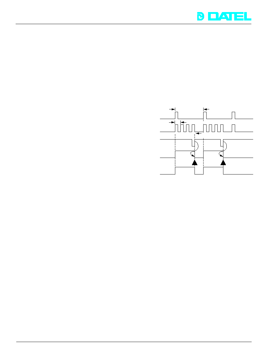
systems, the DVME-614 operates in many modes. Figure 2
shows multiple trigger configurations with the Acquire flag as
an A/D converter clock gate. Triggering may be from internal
or external clocks or from the analog comparator. For precise
phase tracking, use both an external trigger and an external
A/D start clock.
Figure 2. Trigger per Scan Mode
Internal or external trigger rate
TRIGGER
START A/D
CONVERT
END OF
SCAN*
(internal signal)
ACQUIRE
FLAG
Maskable
Interrupt
and Status
0
1
2
3
Internal or external start rate
Fixed or sequential channel addressing up to
64k samples per trigger
SSH (Internal)
[BASE + 2 bit 6 = 1]
HOLD
SAMPLE
A/D Data Format
A/D data is delivered as a stream from the FIFO memory. For
multichannel inputs, this means that data is multiplexed by the
channel address with a modulo address wrap-around at the
top channel. For example, with 4-channel inputs, the output
channel sequence is 0, 1, 2, 3, 0, 1, . . .
Note that all A/D data is right-justified within the 16-bit data
word with sign extension to bit 15.
168

DVME-614
Æ
Æ
DATEL, Inc., Mansfield, MA 02048 (USA)
∑
Tel: (508)339-3000, (800)233-2765 Fax: (508)339-6356
∑
Email: sales@datel.com
∑
Internet: www.datel.com
FUNCTIONAL SPECIFICATIONS
(Typical at +25∞C, dynamic conditions, gain = 1, unless noted)
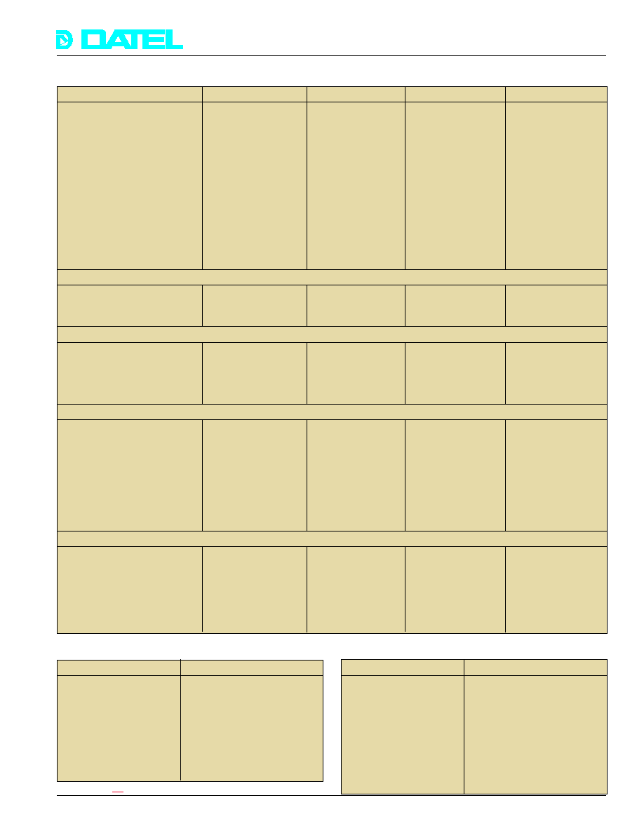
DVME-614F
2 Simultaneous
Single Ended
0 to +10 V
±5 V
±15 V
2 µs
--
>1 M
165 ns
20 ns
±40 ps
12 bits
400 ns
2
±1
±1
±0.1
±0.1
2 MHz
2 MHz/chan.
≠70 dB
DVME-614E
16SE/8D
SE or Diff.
0 to +10 V
±10 V
±5 V
±15 V
2 µs
±10 V
100 M
750 ns
20 ns
±40 ps
12 bits
500 ns
1
±1
±0.75
±0.1
±0.1
2 MHz
500 KHz
≠72 dB
DVME-614B
4
Single Ended
0 to +10 V
±10 V
±5 V
±15 V
2 µs
--
10 M
750 ns
20 ns
±100 ps
14 bits
1.6 µs
1
±1.5
±1
±0.3
±0.3
500 KHz
330 KHz
≠75 dB
ANALOG INPUTS
Number of Channels
Input Configuration
(non-isolated) [Note 19]
Full Scale Input Ranges
(user-selectable) (gain =1)
[Notes 1 and 16]
Input Overvoltage
(no damage, power on)
Overvoltage Recovery
Time, maximum
Common Mode Voltage
Range, maximum
Input Impedance
[Notes 6 and 9]
Acquisition Time
Aperture Delay
Aperture Delay Uncertainty
Resolution
Conversion Period
Number of A/D Converters
Integral Non-linearity
(LSB of FSR)
Differential Non-linearity
(LSB of FSR)
Full Scale Temperature
Coefficient (LSB per ∞C)
Zero or Offset
Temperature Coefficient
(LSB per ∞C)
Sample Rate
(single channel only)
Sample Rate per Channel
(simul. or sequential chans.)
[Note 4]
Total Harmonic Distortion
[Note 3]
DVME-614D
1
Differential
±5 V
±15 V
2 µs
±1 V
2 K
50 ns
10 ns
±7 ps
12 bits
200 ns
1
±2
±1
±0.1
±0.3
5 MHz [6]
--
≠68 dB
SAMPLE/HOLD
A/D CONVERTER
SYSTEM DC CHARACTERISTICS [Note 7]
SYSTEM DYNAMIC PERFORMANCE [Notes 2 and 3]
Note:
Model DVME-614J in short-cycled addressing is recommended in place of the DVME-614A.
Model DVME-614E can substitute for the DVME-614C.
ANALOG INPUTS
Programmable Gains
See Note 1
Common Mode Rejection
(DC - 60 Hz)
-80 dB (g = 100) (416E)
Addressing Modes
1. Single channel
(short cycle channel
2. Simultaneous sampling
addressing is software-
3. Sequential with
selectable on
autosequenced addressing
DVME-614J,L)
4. Random addressing by host
software
A/D CONVERTER
Output Coding
Positive-true, right justified,
straight bin. (unipolar) or right-
justified 2's comp. (bipolar) with
sign extension thru bit 15
Trigger Sources
1. Local Pacer frame clock
(Software selectable)
2. External TTL frame clock
3. Analog threshold comp.
A/D Sample Clock
1. Internal programmable
82C54 timer
2. Ext. TTL input, active high
Please read all notes carefully.
169

DVME-614
Æ
Æ
DATEL, Inc., Mansfield, MA 02048 (USA)
∑
Tel: (508)339-3000, (800)233-2765 Fax: (508)339-6356
∑
Email: sales@datel.com
∑
Internet: www.datel.com
ANALOG INPUTS
Number of Channels
Input Configuration
(non-isolated) [Note 19]
Full Scale Input Ranges
(user-selectable) (gain =1)
[Notes 1 and 16]
Input Overvoltage
(no damage, power on)
Overvoltage Recovery
Time, maximum
Common Mode Voltage
Range, maximum
Input Impedance
[Notes 6 and 9]
Acquisition Time
Aperture Delay
Aperture Delay Uncertainty
Resolution
Conversion Period
Number of A/D Converters
Integral Non-linearity
(LSB of FSR)
Differential Non-linearity
(LSB of FSR)
Full Scale Temperature
Coefficient (LSB per ∞C)
Zero or Offset
Temperature Coefficient
(LSB per ∞C)
Sample Rate
(single channel only)
Sample Rate per Channel
(simul. or sequential chans.)
[Note 4]
Total Harmonic Distortion
[Note 3]
FUNCTIONAL SPECIFICATIONS
(Typical at +25∞C, dynamic conditions, gain = 1, unless noted)
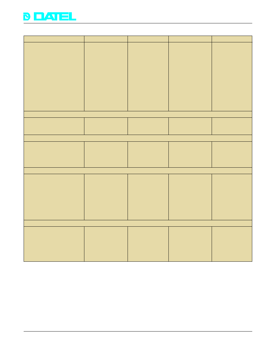
DVME-614K
2 Simultaneous
Limited Differential
0 to +10 V, ±5 V
(separate models)
±15 V
--
±1 V
1 K
50 ns
10 ns
±7 ps
12 bits
200 ns
2
±2
±1
±0.1
±0.3
5 MHz
5 MHz/ch.
≠68 dB
DVME-614G
2 Simultaneous
Single Ended
±5 V or
0 to +10 V
(separate models)
±15 V
2 µs
--
>1 M
350 ns
20 ns
±70 ps
14 bits
1 µsec*
2
±1.5
±1
±0.3
±0.3
1 MHz*
1 MHz/chan.*
≠80 dB
DVME-614H
1
Differential
±5 V
(other ranges
special order)
±15 V
1 µs
±1 V
2 K
35 ns
±10 ns
3 ps rms
12 bits
100 ns
1
±1.5
±1
±1
±1
10 MHz
--
≠65 dB
DVME-614J
8 Simultaneous
Single Ended
±5 V, ±10 V
[Note 10]
±15 V
--
--
8 K
(bipolar)
400 ns
--
--
12 bits
2 µs
(all chans. in
simul. sampling)
8
±1
±1
[Note 10]
[Note 10]
400 KHz
250 KHz/chan.**
≠75 dB
SAMPLE/HOLD
A/D CONVERTER
SYSTEM DC CHARACTERISTICS [Note 7]
SYSTEM DYNAMIC PERFORMANCE [Notes 2 and 3]
*Dual 2 MHz 14-bit sampling is available on special order.
**A 380 KHz/channel option is available on special order.
170

DVME-614
Æ
Æ
DATEL, Inc., Mansfield, MA 02048 (USA)
∑
Tel: (508)339-3000, (800)233-2765 Fax: (508)339-6356
∑
Email: sales@datel.com
∑
Internet: www.datel.com
FUNCTIONAL SPECIFICATIONS
(Typical at +25∞C, dynamic conditions, gain = 1, unless noted)
ANALOG INPUTS
Number of Channels
Input Configuration
(non-isolated) [Note 19]
Full Scale Input Ranges
(user-selectable) (gain =1)
[Notes 1 and 16]
Input Overvoltage
(no damage, power on)
Overvoltage Recovery
Time, maximum
Common Mode Voltage
Range, maximum
Input Impedance
[Notes 6 and 9]
Acquisition Time
Aperture Delay
Aperture Delay Uncertainty
Resolution
Conversion Period
Number of A/D Converters
Integral Non-linearity
(LSB of FSR)
Differential Non-linearity
(LSB of FSR)
Full Scale Temperature
Coefficient (LSB per ∞C)
Zero or Offset
Temperature Coefficient
(LSB per ∞C)
Sample Rate
(single channel only)
Sample Rate per Channel
(simul. or sequential chans.)
[Note 4]
Total Harmonic Distortion
[Note 3]
DVME-614L
16 Simultaneous
Single Ended
±5 V, ±10 V,
(user selectable)
[Note 10]
±15 V
--
--
8 K
400 ns
--
--
12 bits
2 µs
(all chans. in
simul. sampling)
16
±2
±1
[Note 10]
[Note 10]
400 KHz
190 KHz/chan.
-75 dB
DVME-614M
4 Simultaneous
Single Ended
±10 V
±12 V
--
--
10 M
--
--
--
16 bits
5 µs
(all chans. in
simul. sampling)
4
±4
±3
±1
±1
200 KHz
200 KHz/chan.
-83 dB
DVME-614N
2 Simultaneous
Single Ended
±2.5 V
±15 V
--
--
10 M
or 50
35 ns
±10 ns
5 ps
14 bits
200 ns
(all chans. in
simul. sampling)
2
±1
±1
±0.5
±0.5
5 MHz
5 MHz/chan.
-75 dB
DVME-614P
4 Simultaneous
A/D's
Single Ended
±2.5 V or
0 to +5 V
(user selectable)
±7 V
--
--
1000
--
--
--
14 bits
400 ns
(all chans. in
simul. sampling)
4
±3
±1.5
±0.5
±0.5
3 MHz* min.
2.5 MHz/chan.
-75 dB
SAMPLE/HOLD
A/D CONVERTER
SYSTEM DYNAMIC PERFORMANCE [Notes 2 and 3]
SYSTEM DC CHARACTERISTICS [Note 7]
* The sample rate to published specifications is 3 MHz. The A/D is functional to 5 MHz. Valid data output per channel is delayed
by 4 samples after the start of the sample clock. Please make note of this for products such as the PC-414P, PC-430P, and
DVME-614P which use non-continuous A/D sampling. Data output is pipelined meaning that the first four samples per channel
should be discarded. For all 4 channels, discard 16 samples. The design is intended for semi-continuous sampling of wideband
signals and is less suitable for low speed data acquisition. Approximately 5 dB SFDR improvement can be achieved by directly
connecting an external A/D sample clock. Contact DATEL for details.
171

DVME-614
Æ
Æ
DATEL, Inc., Mansfield, MA 02048 (USA)
∑
Tel: (508)339-3000, (800)233-2765 Fax: (508)339-6356
∑
Email: sales@datel.com
∑
Internet: www.datel.com
SPECIFICATIONS, CONTINUED
(Typical @ +25∞C, dynamic conditions, unless noted)
A/D MEMORY
Architecture
First-In, First-Out (FIFO)
Memory Capacity
1024, 4096, or 16,384 A/D
samples
Programmable Interval
Timer Type
82C54
Functions
1. A/D EOC sample count.
2. A/D start rate (16-bit
divisor) 4MHz max. on-
board.
3. Scan or frame rate of 3 to
65,536 samples. Drives
the Acquire flag/interrupt
gate for A/D start pulses.
82C54 Clock Source
1. Internal 8MHz crystal
(user selectable)
clock derived from
VMEbus SYSCLK.
2. External BNC TTL input,
10MHz maximum.
Scan Trigger Clock
125, 250, or 500kHz
Analog Trigger Input Range
±10V (not avail. on 614D).
Analog Trigger Response
2µs to set status flag
Analog Trigger Hysteresis
±40mV
Number of Channels
One channel
Function
1. General purpose analog
(user selectable)
output
[Footnotes 5 and 20]
2. Threshold to comparator
for analog trigger
Resolution
12 bits
Output Voltage Range
0 to +10V, ±5V, and ±10V at
(user selectable)
5mA maximum.
Linearity
±0.05% of FSR
Settling Time
(10V step)
5 microseconds to 0.05%
Input Coding
Straight binary
Standards Compliance
IEEE P1014/D1.0
Data Bus Width
16 bits using P1 connector.
Address Bus
24 address lines (A23-A01)
plus 6 address modifiers.
Address Modifier Codes
39 hex or 3D hex, selectable.
VMEbus Interrupt
1 line, selectable IRQ 1-7.
Asserts maskable
programmable 8-bit vector
ID code.
Architecture
SAD24:SD16 slave consisting
of 16 contiguous word
registers.
Bus Interrupt Sources
Scan acquire flag (sample
count), FIFO full or half full.
Control/Status Functions
FIFO reset, FIFO flags,
interrupt select/status, trigger
source, timer control/period,
sample count load, parallel
outport transfer status, A/D
enable, MUX autosequence.
Data Transfer
Uses 16MHz VMEbus
SYSCLK signal to generate
DTACK* with selectable delay.
Parallel Outport
16 lines, TTL levels from FIFO.
Includes ready out,
acknowledge in, and transfer
enable in handshakes.
Outport steering is software
enabled.
Function
Asynchronous slave to
remote master. Does not
provide addressing. All data
is sequential. The transfer
enable input from a remote
master is displayed as a
status bit.
Parallel Port Loading
24mA out, 1.6mA in.
Parallel Port Data Rate
4MHz max. to external
processor.
VMEbus, P1
96-pin male DIN connector.
The P2 connector is not used.
Analog Input Connectors
Four BNC bayonet coaxial
mounted on front panel.
DB-25 used for 614E, J, L.
Multipurpose Connector
5th BNC user-selectable for:
a) Pacer trigger input
b) Analog threshold
comparator input.
c) D/A output
Parallel Port
Front panel 25-pin female
DB-25S. Provides external
clock in.
Power Required
+5V, ±5% at 3.0A max. from
VMEbus.
Operating Temp. Range
0 to +60∞C. Forced cooling
is required.
Storage Temp. Range
≠20 to +80∞C
Relative Humidity
10 to 90%, non-condensing.
Altitude
0 to 10,000 feet.
Outline Dimensions
Double height VME, 6U outline.
9.19"W x 6.3"D x 0.6"H
(233.5 x 160 x 15.24 mm).
Weight
17 ounces (482 grams).
Analog Section Modularity
The MUX-S/H-A/D module is
socketed for function
interchange.
Analog Adjustments
Offset and gain pots provided
on DVME-614B,C,D,E,F,G,M,P
Note: 16MHz VMEbus SYSCLK is
required.
TRIGGER CONTROL
PARALLEL DATA PORT
MISCELLANEOUS
CONNECTORS
ANALOG OUTPUT
VMEbus INTERFACE
172

DVME-614
Æ
Æ
DATEL, Inc., Mansfield, MA 02048 (USA)
∑
Tel: (508)339-3000, (800)233-2765 Fax: (508)339-6356
∑
Email: sales@datel.com
∑
Internet: www.datel.com
13. DVME-614J and L bipolar input is user-selectable ±5V or
±10V per channel (default). Total gain error over
temperature range is ±4LSB maximum. Total zero/offset
error oever temperature range is ±4LSB maximum.
Monotonicity: no missing codes over temperature range.
14. DVME-614G acquisition time is 350ns to ±0.003% of FSR.
15. Models DVME-614D, H, K, and M use a single channel
12-bit A/D converter with ±5V inputs. An external A/D
clock is required above 4MHz and the 82C54 timer must
be bypassed. 10MHz sampling may continue until the
FIFO memory is full.
16. Input polarity. Some models are fixed as bipolar only
whereas others are user-selectable unipolar or bipolar.
Still others require separate model numbers.
17. Models F, G, J, K, L, M, N, and P use one A/D converter
per channel.
18. The customer must supply shielded cables and a
certified computer to insure EMC compliance.
19. A/D-per-channel boards (models F, G, J, K, L, M, N, P)
may be operated in "software differential" mode. Two A/D's
are applied to the high and low legs of a single differential
input channel. The two data values are then algebraically
subtracted, either on the fly in real time or after all
samples have been stored. Channel capacity in "software
differential" is one-half the number of single-ended
channels.
This technique offers excellent bandwidth, high common
mode rejection and optional mix of single-ended and
differential channels.
20. There is no D/A channel on DVME-614D.
NOTES
1.
Resistor-programmed gain (user supplied) from X1 to
X100 is available on DVME-614E with increased settling
delay at higher gains. Requires precision gain resistor.
2.
Total throughput includes MUX settling time after
changing the channel address, S/H acquisition time to
rated specifications, A/D conversion, and FIFO transfer.
Total throughput is not delayed by host software
whenever the FIFO is not full.
3.
THD test conditions are:
1. Input freq.
500kHz (614F)
200kHz (614B,E,G)
50kHz (614J,L,M)
1MHz (614D,K)
2MHz (614H)
2. Generator/filter THD is -90dB minimum.
3. THD computed by FFT to 5th harmonic.
( V2
2
+ V3
2
+ V4
2
+ V5
2
)
0.5
Vin
4. Inputs are full scale less 0.5dB. No channel advance.
5. A/D sample rate = 500kHz (614B,E,G), 5MHz (614D,K),
2MHz (614F), 10MHz (614H), 250kHz (614J),
190kHz (614L,M)
6. Crystal oscillator is used.
4.
The rates shown for sequential sampling are the
maximum A/D converter start rates and include MUX
sequencing and settling. For example, if four channels
of the DVME-614E were scanned, the maximum sample
rate on any one channel would be 2µs x 4 channels =
8µs (125kHz per channel).
5.
For fastest response on the analog comparator trigger,
keep the reference voltage near the trip input voltage. To
avoid overload recovery delays, do not let the trip input
(or any other analog input) exceed ±10V.
6.
The input impedance of 10M
minimum avoids
attenuation errors from external source resistance. For
many applications, an in-line coaxial 50
shunt, inserted
adjacent to the front connectors, is recommended to
reduce reflections and standing wave errors.
7.
Allow 20 minutes warmup time to rated specifications for
models DVME-614B,G,M,N.
8.
A 25-pin DB-25S connector is used for the DVME-614E,J,L.
9.
Input impedance is shown with power on. Impedance
with power off is 1500 Ohms or less.
10. Full power bandwidth is shown at approximately 3%
distortion level. This is not the ≠3dB amplitude response
which is at a higher but non-Nyquist frequency.
11. Avoid mixing external triggers which are a close
submultiple of the internal A/D start clock to prevent
lost samples.
12. The 5th coaxial connector may be dedicated to either
external trigger or external A/D clock.
log10
( )
THD = 20
Register Memory Mapping
The base address may be selected anywhere up to $FFFF00h
on 32-byte boundaries.
Address
(hex)
Direction
Description
BASE + 0
Write
Command Register
BASE + 0
Read
Status Register
BASE + 2
Write
Channel Address Register
BASE + 4
Write
D/A Data Register
BASE + 6
Write
FIFO Reset Register
BASE + 8
Not used
BASE + 0Ah
Not used
BASE + 0Ch
Read/Write
Interrupt Vector ID
BASE + 0Eh
Read
FIFO A/D Data Register
BASE + 10h
Read/Write
Counter #0 (82C54)
BASE + 12h
Read/Write
Counter #1 (82C54)
BASE + 14h
Read/Write
Counter #2 (82C54)
BASE + 16h
Read/Write
Control Register (82C54)
At power-up or VMEbus reset, all registers contain zeroes
except the FIFO HF and FF bits. The registers may be
programmed in any sequence as long as the command
register is last. See user manual for full details.
173

DVME-614
Æ
Æ
DATEL, Inc., Mansfield, MA 02048 (USA)
∑
Tel: (508)339-3000, (800)233-2765 Fax: (508)339-6356
∑
Email: sales@datel.com
∑
Internet: www.datel.com
Input Channels, A/D Resolution
B = 4SE chans., 14 bits
J = 8SE simul. chans., 12 bits
D = 1D chan., 12 bits
K = 2SE simul. chans., 12 bits
E = 16SE/8D chans., 12 bits
L = 16SE simul. chans., 12 bits
F = 2SE simul. chans., 12 bits
M = 4SE simul. chans., 16 bits
G = 2SE simul. chans., 14 bits
N = 2SE simul. chans., 14 bits
H = 1D chan., 12 bits
P = 4SE simul. chans., 14 bits
FIFO Memory Size
1 = 1,024 A/D samples
2 = 4,096 A/D samples
3 = 16,384 A/D samples
Input Range Polarity
A = Bipolar or selectable
B = Unipolar
Use the "A" designator for
all models with user-
selectable input polarity.
CAUTION: Read the input
range specs carefully.
DVME-614
ORDERING INFORMATION
A software disk and user manual are included. Boards are power-cycle burn-in tested.
DVME-691
Screw terminal signal conditioning panel, pin-compatible to DVME-614E, J, and L.
Example: DVME-614F3 Two simultaneous A/D's, 2MHz, 12-bit resolution, 16,384 FIFO samples.
Hardware:
Array Pre-processing
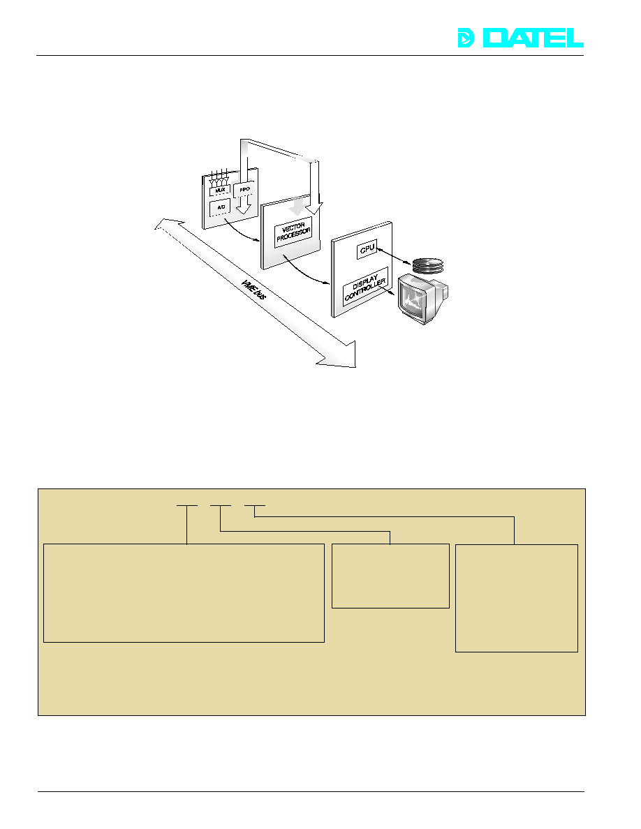
Figure 4 shows the DVME-614 installed in a typical VME application. The DVME-614 may be connected to an array processor board
via a parallel port or the VMEbus. The parallel port offers higher speed by offloading block data transfers from the VMEbus. A
separate cable is required for the parallel port.
ANALOG INPUTS
4 SSH CIRCUITS
BINARY A/D DATA
MASS STORAGE
GRAPHICS DISPLAY
PARALLEL PORT
DVME-614
A/D BOARD
ARRAY PROCESSOR or
PARALLEL RECEIVER
CPU, MEMORY, DISK I/O
DSP ARRAYS
Figure 4. Array Pre-processing with the DVME-614
174
