PC-411/412
16-Channel, Analog I/O Boards
with FIFO for IBM-PC Computers
PRODUCT DATA
Æ
Æ
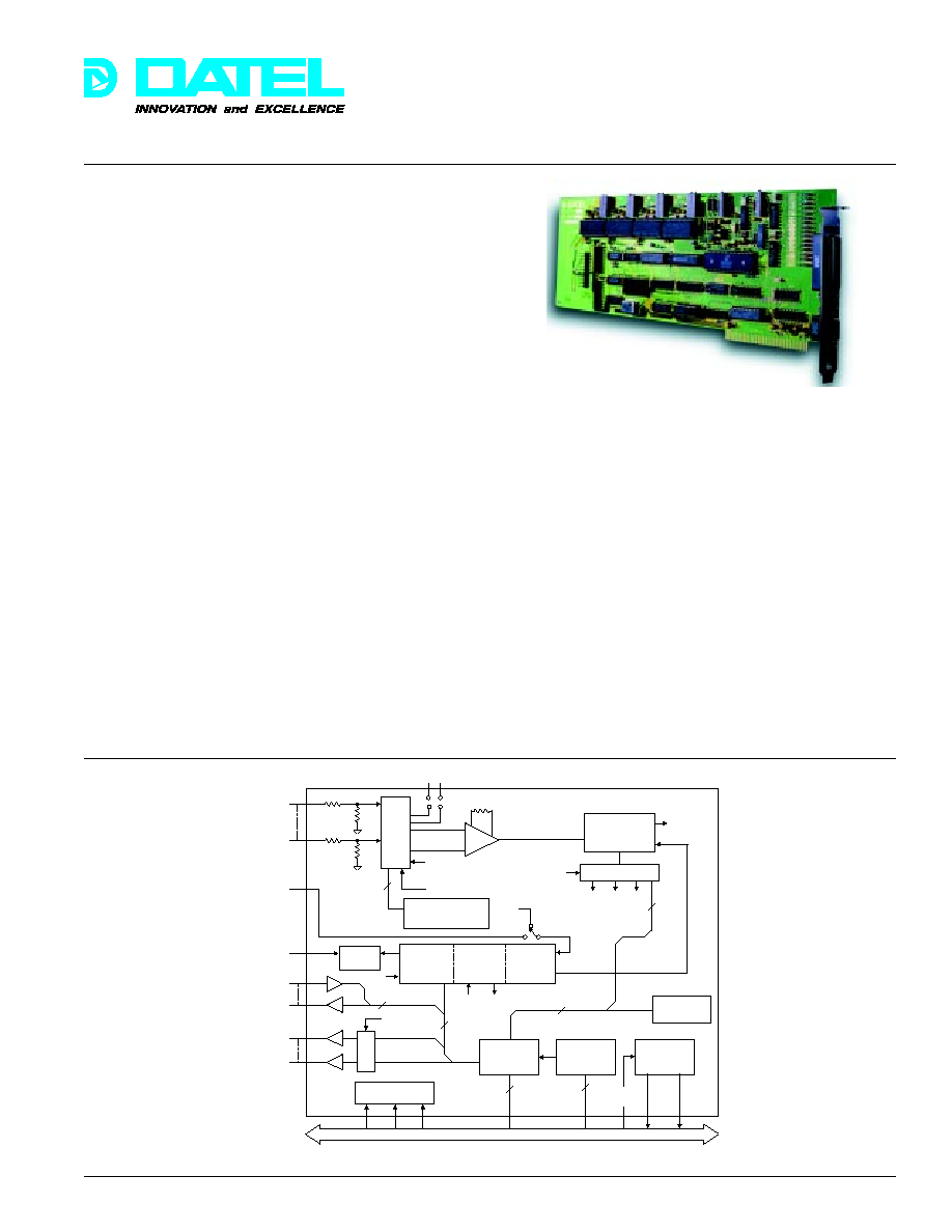
Figure 1. PC-411/412 Block Diagram
FEATURES
∑∑
∑∑
∑
16SE or 8D analog input channels, expandable to 256
∑∑
∑∑
∑
4 Analog output channels optional (PC-412) with
simultaneous update
∑∑
∑∑
∑
Choice of 12, 14, or 16-bit A/D resolution
∑∑
∑∑
∑
On-board programmable trigger clock
∑∑
∑∑
∑
Discrete digital I/O (8 input, 8 output)
∑∑
∑∑
∑
FIFO memory, DMA, and programmable interrupts for
continuous, non-stop, "streaming" data acquisition
∑∑
∑∑
∑
Programmable gain amplifier
∑∑
∑∑
∑
Signal conditioning per channel
Offering non-stop continuous collection of up to 16 analog
input signals in real time, the PC-411 is an analog input board
for IBM-PC, PC/XT, PC/AT, and compatible computers. The
PC-411 accepts 16 single-ended or 8 differential input signals,
digitizes them up to 12, 14, or 16-bit resolution and places
them on the computer bus under software control. Data may
then be stored in PC memory, saved on disk, or displayed on
the screen or printer.
Model PC-412 is a combination analog input and output board
using the same input section as the PC-411. The PC-412 adds
four optional analog output channels to be used for chart
recorders, actuator controllers, or other output devices. Both the
PC-411 and PC-412 accept external analog input expansion
channels. On both the PC-411 and PC-412, sixteen discrete
digital I/O lines are configured as 8 inputs and 8 outputs for
external logic devices. The digital outputs can control the
channel addressing of an expansion input multiplexer.
The differential analog inputs offer rejection of common mode
noise while the on-board Programmable gain amplifier (PGA)
offers higher gains (up to times 100) for low-level sensors. On-
board circuit pads on each channel may be configured for other
input voltage or current ranges or input signal conditioning.
Analog-to-digital converter (A/D) data passes to an on-board
First-In, First-Out (FIFO) data memory. FIFO data is then
transferred to the host computer bus interface under software
control. Besides temporarily storing a block of samples, the
FIFO acts to decouple the precise timing of the A/D section
from the block-oriented data transfer burst on the bus.
Unlike many other analog input boards for the PC, the
PC-411/412 can continuously collect analog data with non-
stop converter triggering while data is simultaneously read by
the PC from the FIFO. This allows the collection of
"seamless" signals of millions of samples or greater. Another
advantage of the FIFO is high-speed disk recording of analog
data with no loss of samples during disk writes.
Expansion up to 256SE/128D total channels is offered on
DATEL's PC-440 MUX board in increments of 32SE/16D
channels.
The timing section controlling the sampling A/D converter is
designed for accurate multi-scan data acquisition. Software
programmable timers control the interval between each
conversion and each multichannel scan. A programmable
sample counter will allow sample blocks of specified length
16SE or 8D
ANALOG
INPUTS
INPUT
EXPANSION
R
GAIN
Reference
Test
Programmable
Gain Amplifier
Sampling A/D
Converter
FIFO Memory
Channel Address
Sequencer
M
U
X
Trigger
Timer
(2)
Sample
Counter
(0)
A/D Start
Timer
(1)
Trigger
Select
Signal
Conditioning
Pads
MUX Enable
1MHz
PC BUS
Simultaneous
Update
31.25
kHz
D/A Converters
Power
Regulators
I/O Bus
Interface
Base Address
Select
Interrupt
and DMA
Request
Control
Registers
EOC
EOS
82C54
EOC
Empty
Half
Full
Start A/D
+5V
+12V
-12V
EXTERNAL A/D
CLOCK IN
EXTERNAL
TRIGGER IN
DIGITAL I/O
(8 IN, 8 OUT)
4 ANALOG
OUTPUTS
(PC-412 only)
Reset
DMA
T/C
CLK
OUT
IRQ
DRQ
DATEL, Inc., Mansfield, MA 02048 (USA)
∑
Tel: (508)339-3000, (800)233-2765 Fax: (508)339-6356
∑
Email: sales@datel.com
∑
Internet: www.datel.com
71

PC-411/412
Æ
Æ
DATEL, Inc., Mansfield, MA 02048 (USA)
∑
Tel: (508)339-3000, (800)233-2765 Fax: (508)339-6356
∑
Email: sales@datel.com
∑
Internet: www.datel.com
A/D CONVERTER CONT.
Output Coding
Positive-true, left-justified,
straight binary (unipolar) or
offset binary (bipolar)
Trigger Sources
1. Local Pacer sample clock
(software-selectable)
2. External digital sample
clock
Addressing Modes
1. Single channel
2. Sequential with
autosequenced addressing
3. Random addressing by
host software
Integral Nonlinearity
±0.05% of FSR (411/412A)
±0.015% of FSR (411/412B)
±0.005% of FSR (411/412C)
Differential Nonlinearity
±0.5 LSB
(±1 LSB 411/412B,C)
Full Scale or Zero/Offset
±0.1 LSB per ∞C (411/412A)
Temp. Coefficient
±0.3 LSB per ∞C (411/412B,C)
Monotonicity
No missing codes
Power Supply Rejection
±0.01% of PC bus ±12V
Total Scan Throughput
17 µs (411/412A)
(sample-to-sample with
23 µs (411/412B)
sequential addressing)
42 µs (411/412C) (see Notes)
Total Throughput
12 µs (PC-411/412A)
(no channel advance)
17 µs (PC-411/412B)
37µs (PC-411/412C)
Architecture
First-In, First-Out (FIFO)
Memory Capacity
512 A/D samples
Programmable Timer/
Counter Type
82C54
Functions
1. EOC sample count
2. A/D start rate (16-bit divisor)
3. Scan or frame rate (16-bit
divisor)
Sample Counter
1 to 65,536 samples. Drives
the acquire flag/interrupt.
A/D Start Clock Source
Internal crystal clock. Range
(software programmable)
500 KHz to 15.26 Hz (16-
stage binary divider or BCD)
Trigger Source
1. Internal crystal clock
(user-selectable)
2. Ext. digital input. TTL levels,
triggers on falling edge
Internal Trigger Range
15.625 KHz to 2.097 sec. (16-
(software programmable)
stage binary divider or BCD)
Number of Channels
4 channels, single-ended
Resolution
12 bits
Output Voltage Range
±5V, jumper selectable per
channel (0 to 10V, ±10V
special order)
Output Current
±5 mA, short circuit protected
Nonlinearity
±0.05% of FSR
Settling Time (full scale step)
5 µs to 0.05% of FSR
Input Coding
Same as input section
Temperature Coefficient
Same as input section
ANALOG INPUTS
Number of Channels
(software selectable)
16SE or 8 diff. channels
Input Channel Expansion
External single-ended or
differential analog inputs
may be accepted using
DATEL's PC-440. Input
characteristics are identical
to the on-board inputs.
Input Configuration
Non-isolated
Full Scale Input Ranges
0 to +5V, ±5V (software
(gain = 1)
selectable). Other voltage
and current ranges are
available with user-installed
precision resistors.
Input Impedance
100 m
, power on,
1.5 K
, power off
Input Bias Current
±200 pA
Input Capacitance
15 pF per channel
Input Overvoltage
±12V max. (no damage)
Overvoltage Recover Time
5 µs
Common Mode Voltage Range
±5V to analog common
Common Mode Rejection
80 dB, dc to 60 Hz, gain = 100
Programmable Gain Amplifier
1 to 100 gains, selectable
by precision gain resistor
(pads provided)
PGA Settling Delay
6 µs to 0.01% (gain = 1)
15 µs to 0.02% (gain = 10)
80 µs to 0.1% (gain = 100)
Resolution
12 bits (PC-411/412A)
14 bits (PC-411/412B)
16 bits (PC-411/412C)
A/D Conversion Period
7 µs (PC-411/412A)
14 µs (PC-411/412B)
32 µs (PC-411/412C)
Aperture Time
25 ns
Acquisition Time
3 µs
FUNCTIONAL SPECIFICATIONS
(Typical at +25∞C, dynamic conditions, unless otherwise noted)
A/D CONVERTER
independent of FIFO length. The timer/counter section uses an
internal clock or an external timebase. The external trigger may
be used to precisely synchronize sampling with external events.
The trigger may start a single sample, a single multi-channel
scan, or "N" multiple scans separated by programmable delays.
Either an interrupt, DMA Request, or status flag indicates
when FIFO data is ready. Normally, a FIFO interrupt from the
PC-411/412 triggers the PC to burst a fixed-length block of
samples to host PC memory. This offers very high overall
system speed by not tying up the bus and allows the PC to
continue with graphics, math, or disk activities.
The PC-412 analog output channels include a simultaneous
update option where all channels drive their outputs to new
values at the same time from a software trigger. Applications
for this include phase-synchronous system simulation,
process control, and coherent field waveform generation.
Most options are software configured, reducing the number of
jumpers required. Window-driven software is available on
MS-DOS disks to configure the board and save data. A
comprehensive user's manual is also included.
A/D MEMORY
TRIGGER CONTROL
INPUT SYSTEM PERFORMANCE
ANALOG OUTPUT
72

PC-411/412
Æ
Æ
DATEL, Inc., Mansfield, MA 02048 (USA)
∑
Tel: (508)339-3000, (800)233-2765 Fax: (508)339-6356
∑
Email: sales@datel.com
∑
Internet: www.datel.com
PC BUS INTERFACE
Architecture
Decodes 16 byte-wide I/O
registers using address
lines A9-A0. Highest base
address is 3F0h.
Data Bus Width
8 bits
PC Bus Interrupt
1 line, software selectable
(software maskable)
IRQ 3, 5, 7.
Bus Interrupt Sources
Scan acquire flag (sample
count). FIFO full, half full
or not empty or DMA T/C.
Bus Data Transfer Rate
1 Mb/sec. or greater,
dependent on host PC
Direct Memory Access
1 line, software-selectable,
DRQ1 or DRQ3 from FIFO
HF, FF, EF, or ACQ
Parallel Outport
8 lines, TTL levels, 24 mA out
Parallel Inport
8 lines, TTL levels, 2 mA in
plus pullup resistor to +5V
Analog Inputs, P1
25-pin female DB-25S
connector on rear mounting
bracket for analog inputs
and trigger
Analog Outputs, P2
9-pin female DB-25S
(PC-412 only)
connector on rear
mounting bracket
Parallel Port
Internal header connector,
0.025 in. pins on 0.100 in.
spacing, suitable for flat cable
PC Bus Connector, P3
Edgeboard connector
Power Required (PC-411)
+5V, ±5% at 1A max. and
±12V, ±5% at 100 mA max.
all supplied from the bus
(PC-412)
+5V: 2A max.
±12V: 250 mA max.
Operating Temp. Range
0 to +60 ∞C forced cooling
recommended
Storage Temp. Range
≠20 to +80 ∞C
Relative Humidity
10% to 90%, non-condensing
Altitude
0 to 10,000 feet
Outline Dimensions
4.2"H x 13.31"L x 0.625"D
(11,43 x 33,81 x 1,59 cm)
compatible to PC bus
Weight
10 oz. (290 grams)
Analog Section Adjustments
Inputs: offset and gain
Outputs: offset and gain
per channel
MISCELLANEOUS
Sampling Rate per Channel
The rates shown for sequential sampling are the maximum A/D
converter start rates and include MUX sequencing and settling
delays. For example, if four channels were scanned, the
maximum sample rate on any one channel of the PC-411/412
would be 17 microseconds times 4 channels, equalling 68
microseconds (14.7 KHz per channel). Observe Nyquist
sample rate rules for inputs with unknown spectral content.
To avoid overload recovery delays, do not let the analog input
exceed the input voltage range.
Highest total system speeds will be achieved if the FIFO is block
transferred using DMA or the REP INS instruction in a loop with
the CX register controlling the count of samples transferred.
Scan
A scan would consist of a group of channels sampled together
with equal delays between each A/D sample, set by the A/D
start clock. A scan is 16S or 8D channels or less. A scan
uses sequential channel addressing.
Frame
Frames are one or more channels sampled together at each
trigger with equal delays between each A/D sample, set by the
A/D start clock. Each frame is started by one trigger. Either
single channel or autosequential scan addressing may be used.
A frame may consist of several contiguous scans with wrap
around addressing. Frames are stopped when the counter 0
Acquire bit is reset to zero.
PROGRAMMING
(Refer to the PC-411/412 user manual for detailed
programming information.)
The BASE address may be selected anywhere up to 3F0h on
16-byte boundaries. At power up or PC bus reset, all registers
contain zeroes except the FIFO HF and FF bits. When settling
one bit in a write only register, remember to select all other bits
according to the desired code. A shadow register should be
considered to store the last value written. The registers may be
programmed in any sequence as long as the command register
is last. "x" bits are don't care or not used.
I/O REGISTER MAPPING
I/O Address
(hex)
Direction
Description
BASE + 0
Write
Command Register
BASE + 0
Read
Status Registers
BASE + 1
Write
Channel Address Register
BASE + 1
Read
FIFO A/D Data Register
BASE + 2
Write
Interrupt/DMA Register
BASE + 2
Read
FIFO Reset Register
BASE + 3
Write
Digital Output Port
BASE + 3
Read
Digital Input Port
BASE + 4
Read/Write
Counter #0 (82C54)
BASE + 5
Read/Write
Counter #1 (82C54)
BASE + 6
Read/Write
Counter #2 (82C54)
BASE + 7
Read/Write
Control Word (82C54)
BASE + 8
Write
DAC 0 low byte
BASE + 9
Write
DAC 0 high byte
BASE + 10
Write
DAC 1 low byte
BASE + 11
Write
DAC 1 high byte
BASE + 12
Write
DAC 2 low byte
BASE + 13
Write
DAC 2 high byte
BASE + 14
Write
DAC 3 low byte
BASE + 15
Write
DAC 3 high byte
NOTES/DEFINITIONS
Input Settling Delays
The PC-411/412 will run faster in single channel operation than
multichannel after the input is settled on the first channel. Total
sample-to-sample throughput time must include input
multiplexer settling time after changing the channel address,
PGA settling time (depending on the gain), sampling A/D
converter acquisition time, and A/D conversion time.
PARALLEL PORT
CONNECTORS
73

PC-411/412
Æ
Æ
DATEL, Inc., Mansfield, MA 02048 (USA)
∑
Tel: (508)339-3000, (800)233-2765 Fax: (508)339-6356
∑
Email: sales@datel.com
∑
Internet: www.datel.com
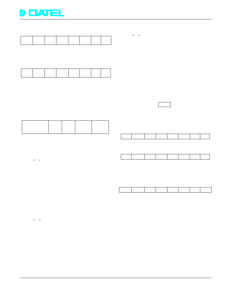
COMMAND REGISTER (Write BASE + 0)
7
6
5
4
3
2
1
0
A/D
Chan.
Read
SE/
Unipolar Auto
A/D
Trig
Calib
Expnd
A/D
Diff
or
Incr
Conv
Int/
Ref
Bipolar
Enbl
Ext
Trigger
0 = Internal trigger from 82C54 timer 2
Select [Bit 0]
1 = External digital trigger
A/D Converter
0 = Disable A/D conversion
Enable [Bit 1]
1 = Enable A/D conversion
Both command bit 1 and the counter 0 ACQuire gate must be
set to enable A/D conversions.
Channel Address
0 = Single channel (no increment)
Autoincrement [Bit 2]
1 = Sequence channel address after
A/D conversion
In an autoincrement, the channel address advances on the A/D
EOC rising edge. For continuous scanning, the address wraps
around to channel 0 after reaching channel 15, modulo 16.
Eight-channel boards wrap after channel 7. Allow adequate
settling time before starting the next A/D conversion. In single-
channel mode, the A/D may be triggered as fast as the EOC
appears.
Unipolar/Bipolar
0 = A/D input range is 0 - 5V
[Bit 3]
1 = A/D input range is ±5V
Single-ended/
0 = Input configuration is single-ended,
Differential [Bit 4]
16 channels
1 = Input configuration is differential,
8 channels
Read A/D Reference
0 = Normal input sampling
[Bit 5]
1 = Select reference input
This bit selects a +4.5V reference channel on the A/D
converter to verify A/D operation. It is not used for calibration.
Input Channel
0 = Enable local channels, disable
Expansion [Bit 6]
expansion inputs.
1 = Disable local channels, enable
expansion inputs.
Bit 6 switches a downstream multiplexer between the local
channel multiplexer and the differential expansion input
channel. If an external user-supplied multiplexer is used for
expansion channels, control external channel addressing
using the parallel digital outputs.
Calibrate A/D
0 = Normal operation
Converter [Bit 7]
1 = Start calibration cycle
Writing a one to this bit then resetting it back to zero begins
an A/D linearization sequence. This takes approximately 20
milliseconds until EOC. Perform this operation once after
power up. During calibration, the A/D converter makes
internal corrections. Periodic calibration is optional in stable
temperature environments but is suggested frequently with
significant temperature changes.
STATUS REGISTER (Read BASE + 0)
7
6
5
4
3
2
1
0
End
FIFO FIFO
FIFO
Acquire
Auto
A/D
Trig
of
Full*
Half
Empty* Status
Incr
Conv
Int/
Conv
Full*
Enbl
Enbl
Ext
Bits 0, 1, and 2 echo the corresponding command register bits
and verify proper register loading.
Acquisition Status
0 = A/D scan not in progress or scan
[Bit 3]
is done. (Counter 0 EOC sample
count was reached.) The A/D is
disabled.
1 = A/D scan in progress. (Counter 0
EOC sample count was not
reached.)
The ACQuire bit resets to zero after a fixed number of
samples (up to 65,536) have been transferred to the FIFO.
The sample count is set by Counter 0. The A/D start clock is
inhibited when ACQ is 0. A special mode allows continuous
non-stop A/D triggering for frames larger than 65K by
counting FIFO transfers in software. ACQ is not valid until the
FIFO starts filling.
FIFO Memory
Bit 4:
0 = FIFO is empty
Status Flags
1 = FIFO is not empty
Bit 5:
0 = FIFO is half full or greater
1 = FIFO is less than half full
Bit 6:
0 = FIFO is full
1 = FIFO is not full
*Note the negative true coding on these bits.
End of A/D
0 = A/D conversion in progress, data
Conversion Status
is invalid
(EOC) [Bit 7]
1 = A/D conversion done, data is valid
Note that all data transfer is through the FIFO. EOC is used
only to monitor the A/D converter. EOC is reset to zero by the
next A/D start convert clock. EOC clocks A/D data into the
FIFO.
INPUT CHANNEL ADDRESS REGISTER (Write BASE + 1)
7 - 4
3 2 1 0
Not
Start
Used
Channel
Address
Start Channel Address
[Bit 3 - 0]
In single-channel mode, these bits select the address of the
next input channel for A/D conversion.
In autoincrement mode, bits 3-0 are the starting channel
address. After each A/D conversion, the EOC automatically
sequences the address. The address wraps around to
channel 0 after reaching channel 15 in single-ended mode or
channel 7 in differential mode. If an exact multiple of 8D or
16S channels is triggered, and the user's program counts
samples, the channel address will not need reloading. The
user must count samples read from the FIFO to determine the
current channel address or must periodically reload the
starting address.
74

PC-411/412
Æ
Æ
DATEL, Inc., Mansfield, MA 02048 (USA)
∑
Tel: (508)339-3000, (800)233-2765 Fax: (508)339-6356
∑
Email: sales@datel.com
∑
Internet: www.datel.com
FIFO A/D REGISTER (Read BASE + 1)
7
6
5
4
3
2
1
0
AD
AD
AD
AD
AD
AD
AD
AD
9
10
11
12
13
14
15
16
LSB
LSB
LSB
12-bit
14-bit
16-bit
versions
versions
versions
Second read:
7
6
5
4
3
2
1
0
AD
AD
AD
AD
AD
AD
AD
AD
1
2
3
4
5
6
7
8
MSB
ALL
A/D data is presented in two sequential reads at the same
output port location. The least significant byte is read first.
The data is left justified and unused least significant bits are
zeroes. Note that A/D data assigns the MSB as A/D bit 1. For
bipolar inputs, the MSB indicates polarity (0 = negative, 1 =
positive).
INTERRUPT CONTROL REGISTER (Write BASE + 2)
7
6
5 4
3 2
1 0
Simultaneous
Not
DMA
Interrupt
Int/DMA
DAC
Used
Level
Level
Source
Update
1 0
1 0
1 0
Hardware flags in the PC-411/412 may cause either an
interrupt or a DMA request. If both an interrupt and DMA are
enabled, an interrupt will be generated by the PC bus DMA
Terminal Count signal only.
Interrupt or DMA Source
Bits
1
0
0
0
= Interrupt request at FIFO full flag.
0
1
= Interrupt request at FIFO half full flag.
1
0
= Interrupt request at Data Acquire flag.
Counter 0 EOC sample count reached.
1
1
= Interrupt or DMA request at FIFO not
empty flag. Each sample will cause a DMA
request if enabled.
This last mode will allow single A/D samples to transfer on
each DMA request. Load the DMA controller count register
with the number of samples to be transferred. When the
Terminal Count is reached, (with optional interrupt) reprogram
the DMA controller then process the previous DMA buffer.
Interrupt Level
Bits
3
2
0
0
= Interrupt disable
0
1
= Interrupt request on the IRQ 3 line
1
0
= Interrupt request on the IRQ 5 line
1
1
= Interrupt request on the IRQ 7 line
DMA Level Select
Bits
5
4
0
0
= DMA disable
0
1
= DMA request on DRQ 1 line
1
0
= DMA request on DRQ 3 line
1
1
= Spare
Only block mode DMA transfers are available (no single
samples).
Simultaneous DAC
0 = Writing to a DAC high byte register
Update [Bit 7]
will update that channel.
1 = All DAC's will simultaneously
update when bit 7 is toggled to
zero then back to one.
If bit 7 = 0, writing to a DAC will not update that channel but
data will be stored for later simultaneous update.
FIFO MEMORY RESET REGISTER (Read BASE + 2)
7 - 0
x - x
Reading this register clears the FIFO and sets the empty flag
true. All previous FIFO data is lost. If A/D conversion is still
running, the FIFO will not be empty when the next A/D EOC
occurs.
DIGITAL OUTPORT REGISTER (Write BASE + 3)
7
6
5
4
3
2
1
0
7
6
5
4
3
2
1
0
Discrete digital outputs are loaded in these bits.
DIGITAL INPORT REGISTER (Read BASE + 3)
7
6
5
4
3
2
1
0
7
6
5
4
3
2
1
0
Discrete digital inputs are read in these bits.
82C54 PROGRAMMABLE INTERVAL TIMER
Counter Register
(Read/Write BASE + 4 - Counter #0)
(Read/Write BASE + 5 - Counter #1)
(Read/Write BASE + 6 - Counter #2)
7
6
5
4
3
2
1
0
C07
C06
C05
C04
C03
C02
C01
C00
Counter 0 counts up to 65,536 A/D samples (load one less
than the desired number of samples). Counter 0 inhibits A/D
conversions when the count is reached. It automatically
reloads the sample count at the next trigger. A special
method is available for non-stop continuous sampling beyond
64K samples (select mode 4 and DO NOT write the counter
registers).
Counter 1 determines the A/D clock rate using a 1 MHz
internal clock or external sample clock.
Counter 2 determines the internal trigger rate between scans
or data frames using a 31.25 KHz internal clock.
75

PC-411/412
Æ
Æ
DATEL, Inc., Mansfield, MA 02048 (USA)
∑
Tel: (508)339-3000, (800)233-2765 Fax: (508)339-6356
∑
Email: sales@datel.com
∑
Internet: www.datel.com
ORDERING GUIDE
Model
A/D Bits
A/D Converter
D/A Channels
Sample Time
PC-411A
12
7 µs
none
PC-411B
14
14 µs
none
PC-411C
16
32 µs
none
PC-412A
12
7 µs
4
PC-412B
14
14 µs
4
PC-412C
16
32 µs
4
Each board is power-cycled burned-in, tested, and calibrated. All models include a user's manual. The warranty period is one
year. Free QuickBASIC or VBASIC disk on request.
PC-411SET
Setup and configuration program. Saves data to disk or memory buffer. Offers calibration and self test.
Supplied on MS-DOS 3.5" and 5.25" disks. Documentation is in the user manual.
PC-411SRC
Source code to PC-411SET on both 5.25" and 3.5" MS-DOS diskettes. Includes "C" and assembly listings
and window library.
PC-412LV, LVS
LabVIEW
Æ
software (see PC-412LV data sheet).
PC-440
Expansion MUX board, 32S/16D channels.
PC-490A/B
Screw termination, PC-490A is 9-pin, PC-490B is 25-pin.
MS-DOS is a trademark of Microsoft Corporation
IBM-PC is a trademark of IBM Corporation
LabVIEW is a trademark of National Instruments
CONTROL WORD REGISTER (Read/Write BASE + 7)
7
6
5
4
3
2
1
0
SC1
SC0
RL1
RL0
M2
M1
M0
BCD
Select Counter
SC1
SC0
0
0
Select counter #0
0
1
Select counter #1
1
0
Select counter #2
1
1
Read back command
Read/Load
RL1
RL0
0
0
Counter latch operation
0
1
Read/Load LSB only
1
0
Read/Load MSB only
1
1
Read/Load LSB then MSB
Mode
M2
M1
M0
x
1
0
Mode 2 rate generator
1
0
0
Mode 4 software strobe
1
0
1
Mode 5 hardware strobe
BCD
BCD
0
16-bit binary count
1
4-decade binary coded decimal count
DAC 0 LOW BYTE (Write BASE + 8)
DAC 1 LOW BYTE (Write BASE + 10)
DAC 2 LOW BYTE (Write BASE + 12)
DAC 3 LOW BYTE (Write BASE + 14)
7
6
5
4
3 2 1 0
DA
DA
DA
DA
Not
9
10
11
12
Used
LSB
DAC 0 HIGH BYTE (Write BASE + 9)
DAC 1 HIGH BYTE (Write BASE +11)
DAC 2 HIGH BYTE (Write BASE + 13)
DAC 3 HIGH BYTE (Write BASE + 15)
7
6
5
4
3
2
1
0
DA
DA
DA
DA
DA
DA
DA
DA
1
2
3
4
5
6
7
8
MSB
DAC data is left justified. With the ±5V bipolar output range,
the MSB is used for polarity (0 = negative, 1 = positive).
In single channel mode (BASE + 2 bit 7 = 0), write the high
data byte last to update all DAC outputs.
A/D CODING TABLE
Input
Input
Output Code
(unipolar)
(bipolar)
(hex)
+ Full scale ≠1 LSB
+Full scale ≠1 LSB
FFF0h
1/2 FS +1 LSB
+1 LSB
8010h
1/2 full scale
Zero
8000h
1/2 FS ≠1 LSB
≠1 LSB
7FF0h
Zero
≠Full scale
0000h
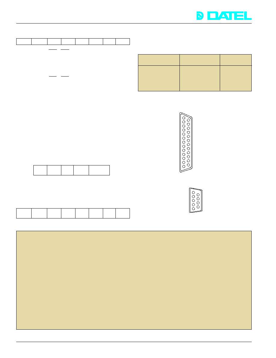
ANALOG SIGNAL CONNECTORS
Pin numbering is shown as viewed from rear panel. (Channel
addresses use single-ended/differential notation.)
Figure 2. Analog Inputs, P1
Figure 3. Analog Outputs, P2
1
2
3
4
5
6
7
8
9
10
11
12
13
CHAN 7 HI
SIGNAL GROUND
CHAN 14 HI/6 LO
CHAN 5 HI
SIGNAL GROUND
CHAN 12 HI/4 LO
CHAN 3 HI
SIGNAL GROUND
CHAN 10 HI/2 LO
CHAN 1 HI
SIGNAL GROUND
CHAN 8 HI/0 LO
EXTRN TRIG* IN
14
15
16
17
18
19
20
21
22
23
24
25
CHAN 15 HI/7 LO
CHAN 6 HI
SIGNAL GROUND
CHAN 13 HI/5 LO
CHAN 4 HI
SIGNAL GROUND
CHAN 11 HI/3 LO
CHAN 2 HI
SIGNAL GROUND
CHAN 9 HI/1 LO
CHAN 0 HI
SIGNAL OR LOGIC GROUND
DAC 3 OUT
DAC 2 OUT
DAC 1 OUT
DAC 0 OUT
EXTRN A/D CLK IN
1
2
3
4
5
6
7
8
9
DAC 0 RETURN
DAC 1 RETURN
DAC 2 RETURN
DAC 3 RETURN
76
