 | –≠–ª–µ–∫—Ç—Ä–æ–Ω–Ω—ã–π –∫–æ–º–ø–æ–Ω–µ–Ω—Ç: PC-422A/B | –°–∫–∞—á–∞—Ç—å:  PDF PDF  ZIP ZIP |

PC-422
Fast Simultaneous 16-Channel
PC/AT Analog Output Board
FEATURES
∑∑
∑∑
∑
8 or 16 analog outputs
∑∑
∑∑
∑
12-bit D/A resolution
∑∑
∑∑
∑
3 microsecond settling time
∑∑
∑∑
∑
Simultaneous update
∑∑
∑∑
∑
Trigger timer interrupt
∑∑
∑∑
∑
Digital I/O (4-In, 4-Out)
∑∑
∑∑
∑
Output ranges selectable per channel
Many applications require phase-synchronous analog outputs.
Examples include precision system simulation and coherent field
generation in process control, audio, acoustics, and sonar. The
PC-422 is a high density analog output board with up to 16 signal
channels. Each Digital to Analog Converter (DAC) channel may
be individually selected for full scale output ranges of 0 to +5V, 0
to +10V, ±5V, or ±10V. All outputs are buffered and will deliver
±0.025% accuracy from 0 to 5 milliamps output load. The PC-
422 is installed in a host IBM-PC/AT or compatible computer.
To achieve the simultaneous update capability, each channel
input register is double buffered. The registers are successively
loaded by the host computer then all channels are updated by
host command or trigger. If preferred, each channel may also be
operated in the non-concurrent transparent mode under program
control with random addressing or single channel operation.
For applications requiring a precision clock to sequence the
output waveforms, the PC-422 includes a software
programmable trigger. The trigger strobes the simultaneous
update and posts a status bit or interrupt to the host PC. Upon
detecting the trigger, the host may block-load the next data
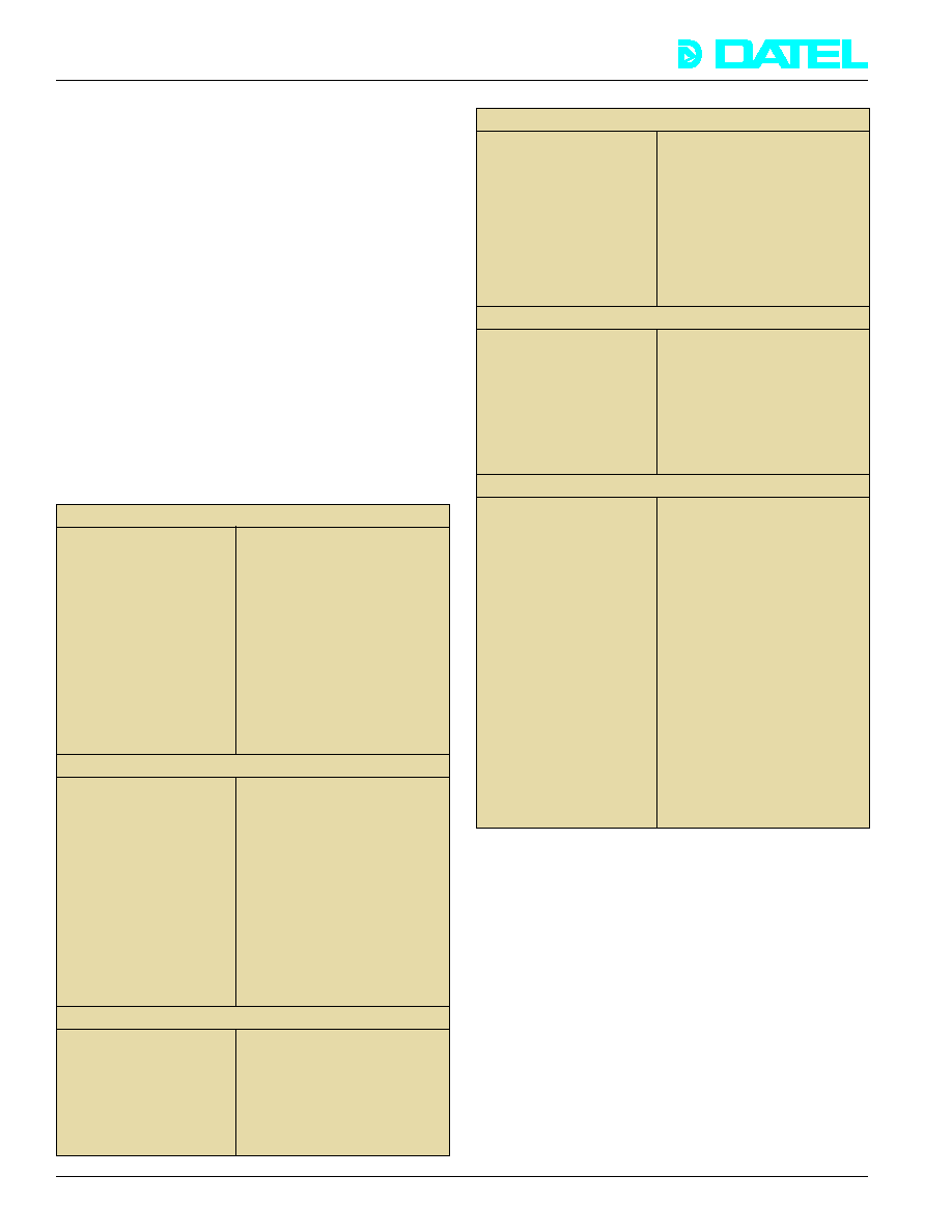
Figure 1. System Block Diagram
PRODUCT DATA
Æ
Æ
frame. The trigger may be derived from an internal crystal
stabilized timer or from an external timer base. The external
trigger option makes the PC-422 fully synchronous with external
events. The trigger section includes a spare output counter,
usable for any purpose.
For repeating frame scan applications, the PC-422 includes an
auto-increment mode. In this mode, block transfer I/O string
instructions will automatically load up to 16 channels at very high
speed from a memory buffer in the PC. The PC-422 will digitally
steer each analog data word to successive DAC input registers
while using the same I/O data register address. The user's
program simply maintains the 80X86 CX register as a
downcounter to terminate each block transfer. Typically, the
trigger and auto-increment modes are used together where the
PC loads the next block after detecting the trigger status signal
from the last simultaneous update.
The combination of a precision frame clock trigger, auto-
increment channel addressing and high speed simultaneous
block loading make the PC-422 ideal for artificial waveform
applications. Such waveform generators continuously loop
8 or 16 Analog Outputs
Digital I/O (4 in, 4 out)
In Out
Spare Counter
External Trigger In
8 MHz
D/A
Converters
Double
Buffers
Simultaneous
Update
Spare
Counter
Internal
Trigger
Timer
82C54
Trigger
Select
Registers
and Control
Logic
Base
Address
Select
I/O Bus
Interface
Interrupt
Request
DC/DC
Power
Converter
DC/DC
Power
Converter
+5V DC
PC/AT Bus
8 Channels
8 Channels
DATEL, Inc., Mansfield, MA 02048 (USA)
∑
Tel: (508)339-3000, (800)233-2765 Fax: (508)339-6356
∑
Email: sales@datel.com
∑
Internet: www.datel.com
123

PC-422
Æ
Æ
DATEL, Inc., Mansfield, MA 02048 (USA)
∑
Tel: (508)339-3000, (800)233-2765 Fax: (508)339-6356
∑
Email: sales@datel.com
∑
Internet: www.datel.com
SPECIFICATIONS, CONTINUED
(Typical @ +25∞C, dynamic conditions, unless noted)
ANALOG OUTPUTS
Number of Channels
8 or 16
Output Configuration
Single-ended, non-isolated
Full Scale Output Ranges
0 to +5V, 0 to +10V, ±5V, ±10V,
individually selectable per channel.
Output Current
0 to ±5 mA min. (source or sink),
short-circuit protected to ground.
Resolution
12 binary bits.
Input Data Coding
Straight or offset binary, positive true
coding. Data is right justified. See
Note 3.
Output Impedance
50 milliohms
Channel Addressing Modes
Random, simultaneous or auto-
increment sequential.
Monotonicity
No missing codes
Linearity Error
(after calibration)
±0.025% of FSR.
Temperature Coefficient
of Gain
±5 ppm typical, ±30 ppm max. of
FSR/∞C max.
Temperature Coefficient of
Zero or Offset
±20 ppm of FSR/∞C max.
Settling Time (FS step)
3 µs max. to ±0.025% of final value
(0 - 5V, 0 - 10V, ±5V ranges).
4µs max. for ±10V range.
Settling Time (1 LSB step)
1 µs to ±0.01%
Slew Rate
10 V/µs minimum
Number of Lines
4 inputs, 4 outputs, non-isolated
Logic Levels
Compatible with TTL, TTL-LS, ALS, etc.
Inputs: "0" <0.8 V, "1" >2.0 V
Outputs: "0" <0.4 V, "1" >2.4 V
I/O Loading
Inputs: 1 LS load plus 10 K
pullup
to +5 V
Outputs: 24 mA source or sink
COUNTER/TIMER
Function
Used as an update strobe for each
multichannel DAC frame.
Frequency Range
2 MHz to 536.87 seconds (32-stage
binary or BCD divider).
Frequency Stability
±50 ppm/∞C
Spare Counter
16-stage binary divider usable for any
purpose. Will divide input signals
from 2 to 65,535. Includes counter
input and output, 1 TTL-LS load,
10 MHz max. input.
Architecture
I/O mapped in 8 contiguous word
locations on 16-byte boundaries.
I/O Mapping
Contains a subset of the local bus,
Decodes I/O address lines A9 through
A4. Maximum base address is 3F0h.
Data Bus
16-bit I/O transfer
Trigger Interrupt
1 interrupt, software-selectable on
level 7, 9, 10, 11, or 15.
Analog Section Adjustments
Full scale gain and zero or offset
potentiometers are provided for each
DAC channel. See Note 2.
Analog Connector [P1]
25-pin DB-25S, also includes the
external trigger input.
Digital I/O Connector [P2]
9-pin DB9S
Spare Timer/Counter
On-board header pins
Operating Temperature Range
0 to +60 ∞C
Storage Temperature Range
≠25 to +85 ∞C
Relative Humidity
10% to 90%, non-condensing
Altitude
0 to 10,000 feet (0 - 3048 m) Forced
cooling recommended.
Power Supply Requirements
+5 V dc, ±5% supplied from PC/AT
bus. 2.5 Amps typ., 4.0 Amps max.
(16 channels), 1.5 Amps typ.,
2.5 Amps max. (8 channels).
Outline Dimensions
4.5"H x 13.31"L x 0.5"W
(11,43 x 33,81 x 1,27 cm)
Weight
1.5 pounds (0,7 Kg)
PERFORMANCE
DIGITAL INPUT/OUTPUT
PC/AT BUS INTERFACE
MISCELLANEOUS
NOTES
1. Depending on the host PC type, I/O transfers may occur
over 1 megasample per second. For example, using the
REP OUTSW instruction, a Compaq 33 MHz 80386 host
achieved approximately 630 nanoseconds instantaneous
sample to sample timing. When estimating system timing,
account for any remaining interrupts required (such as the
real time clock) and DDRAM refresh delays, if any.
2. Recalibration is recommended at 90 day intervals,
depending on conditions.
3. All DAC input registers reset to zero or half-scale (0800h)
at power-up or bus reset, depending on the unipolar/
bipolar switch selection.
through a large RAM buffer containing a synthetic composite
digitized analog signal.
Fast settling rates are another feature of the PC-422. Full scale
step response of each DAC channel is 3 microseconds. Block
transfers of input data may occur faster than individual DAC
channel analog settling times. Each DAC channel input register
can be updated at over 1 megasample per second.
The PC-422 is configured on a PC/AT compatible board
measuring 4.5 inches high by 13.31 inches long. Analog signal
connections are made using a rear panel 25-pin "D" connector.
Eight digital channels (4 inputs and 4 outputs) of discrete I/O are
provided for general purpose control and monitoring of external
logic devices. A 9-pin "D" connector provides digital I/O. The PC-
422 includes tow high efficiency DC to DC power converters to
supply local analog circuits. The entire board uses only +5V DC
power from the PC/AT bus. The board is compatible with all
popular computer languages although the highest speed will
require assembly language. A comprehensive user's manual is
included with the board showing full programming and
application information.
124

PC-422
Æ
Æ
DATEL, Inc., 11 Cabot Boulevard, Mansfield, MA 02048-1151 (U.S.A.) ∑ Tel: (508) 339-3000, (800) 233-2765 Fax: (508) 339-6356 ∑ Email: sales@datel.com
Programming Notes
There are three ways to cause an update of the DAC
registers. Either a register write may be used, or the internal
trigger clock or an external digital trigger input.
To load multiple scans from a large host memory array, use
the following sequence:
Program the channel address register for the starting address.
Program the command register for auto-increment and trigger
updating. Load the first scan into the data channels. Your
load program will have to count the number of loads then exit.
1.
Poll the status register to detect the trigger. If the trigger
was not received, continue polling.
2.
When the trigger occurs, optionally test the overrun flag
and report any errors. To save time, overrun testing may
be deleted if you are sure not data was lost.
3.
When the trigger occurs, block load the next data scan
while advancing the PC's buffer memory address pointer.
For the highest speed, use the 80X86 CX register or
other index as a downcounter to terminate the load. Also,
if this is a circular host buffer, remember to wrap the
pointer to the bottom of the buffer when it reaches the
top.
4.
If the DAC channel address did not wrap around exactly
to channel zero, write the new start channel address.
5.
Write to the simultaneous update register to arm the
trigger update ready flag.
6.
If more scans are needed, go to step 1.
Trigger status polling should be used for the very highest
speed. If somewhat lower update rates are needed, DAC
refresh may use either the trigger interrupt or by polling. The
trigger interrupt is especially useful if other system tasks are
concurrent, such as disk I/O or graphics screen writes.
I/O Register Mapping
The base address may be selected anywhere up to 3F0h on
16-byte boundaries. At power-up or PC bus reset, all control
registers contain zeroes. The DAC data register should be
programmed after setting up the channel address and
command mode. The 82C54 registers must be programmed
in a specific sequence, discussed in the user manual. 16-bit
I/O word instructions must be used. Unlisted registers are not
used.
I/O Address
Direction
Description
(hex)
BASE + 0
Write
Command Status
BASE + 0
Read
Status Register
BASE + 2
Write
DAC Channel Address Register
BASE + 4
Write
DAC Data Register
BASE + 6
Write
Simultaneous Update Register
BASE + 8
Read/Write
Counter 0 (82C54)
BASE + 0Ah
Read/Write
Counter 1 (82C54)
BASE + 0Ch
Read/Write
Counter 2 (82C54)
BASE + 0Eh
Read/Write
Control Word Register (82C54)
Note: "x" bits are "don't care".
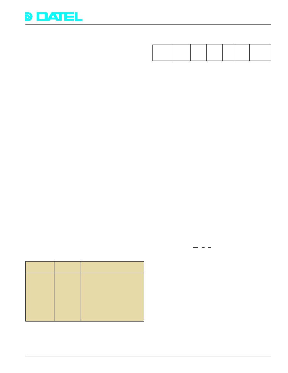
Command Register (Write I/O BASE + 0)
15 - 11
10 9 8
7
6
5
4
3 2 1 0
Not
Intrpt
Simul
Simul
Ext/
Chan
Digital
Used
Level
Updt
Updt
Int
Auto
Outport
2 1 0
Sel
Mode
Trig
Incr
3 2 1 0
Digital Outport
Discrete digital outputs are written to
[Bits 3, 2, 1, 0]
these bits.
Channel Address
0 = No channel increment
Auto-increment [Bit 4]
1 = Increment channel address after
a DAC data register write.
In the non-increment mode (bit 4 = 0), successive writes to
the DAC data register will load into a single DAC channel
selected by the last address written into the channel address
register.
In auto-increment mode (bit 4 + 1), the channel address will
advance after each data register write. The address will cycle
around to channel 0 after reaching channel 15, modulo 16.
Trigger Source Select
0 = Internal trigger
[Bit 5]
1 = External trigger
The trigger may be supplied either from the internal clock
(counters 0 and 1) or from an external digital trigger input. In
the update mode (bit 6 = 1, bit 7 = 1), the trigger strobes all
DAC channels simultaneously from previously written DAC
data.
Simultaneous Update
0 = Update via the simultaneous
Mode [Bit 7]
update register (Write BASE + 6).
1 = Update via internal or external
trigger.
Simultaneous update causes all 8 or 16 DAC channels to be
loaded with data that was last written to their input registers.
If command bit 6 = 0, the trigger will be inhibited.
Simultaneous Update
0 = Transparent mode (immediate
Select [Bit 7]
DAC conversion of input data)
1 = Hold data until update
With bit 7 = 0, DAC analog outputs will follow their input data
values as fast as those values are written. If bit 7 = 1,
updating the DAC outputs will wait until the trigger or a write to
the update register.
Interrupt Level
Bit 10 9
8
Select
0
0
0
= No interrupt
0
0
1
= Interrupt Request Level 7
0
1
0
= Interrupt Request Level 9
0
1
1
= Interrupt Request Level 10
1
0
0
= Interrupt Request Level 11
1
0
1
= Interrupt Request Level 15
1
1
0
= No interrupt
1
1
1
= No interrupt
These bits select the IRQ line on the PC/AT bus where trigger
interrupts are placed.
125

PC-422
Æ
Æ
DATEL, Inc., Mansfield, MA 02048 (USA)
∑
Tel: (508)339-3000, (800)233-2765 Fax: (508)339-6356
∑
Email: sales@datel.com
∑
Internet: www.datel.com
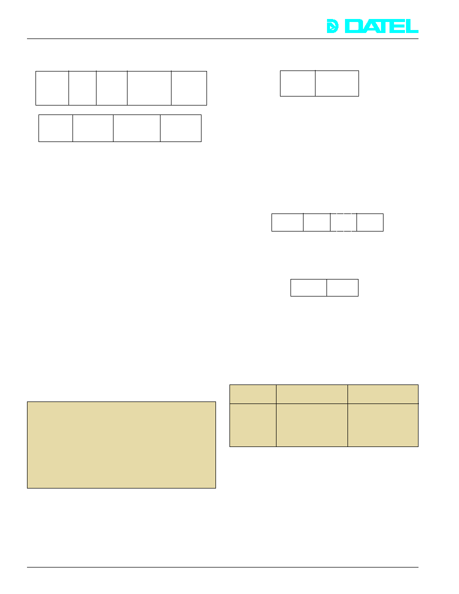
Status Register (Read I/O BASE + 0)
15
14
13 12
11 - 8
7
Update
Over
Not
Current
Simul.
Ready
Run
Used
Channel
Update
Status
Error
Address
Select
X X
3 2 1 0
6
5
4
3 2 1 0
Simul.
External/
Chan Addrs
Digital
Update
Internal
Auto
Inport
Mode
Trigger
Increment
3 2 1 0
Digital Inport
Discrete digital inputs may be read in
[Bits 3, 2, 1, 0]
these bits.
Status Bits
These bits follow the corresponding
[Bits 7 - 4]
bits in the command register.
Current Channel
These bits indicate either the last
Address [Bits 11 - 8]
address written into the channel
address register or the next channel
address to be written to by the next
DAC data write.
These addresses will sequence from
channel 0 to 15, modulo 16 in auto-
increment mode.
Overrun Error
In trigger update mode (command 6 =
[Bit 14]
1) this bit will be set to one if a trigger
occurs before the next load of the DAC
data register. Any write to the
command register resets bit 14 to zero.
Update Ready
With command bit 7 = 1, a write to the
Status [Bit 15]
simultaneous update register will set bit
15 to one. The trigger will reset this bit
to 0, indicating that the next frame of
data may be loaded. If a trigger occurs
before bit 15 is set to 1, the overrun
error bit will be set to 1.
Bit 15 is normally polled to detect the
trigger after loading the data registers.
Bit 15 is normally polled to detect the
trigger after loading the data registers.
Bit 15 stays at 0 if command bit 6 = 0.
Ordering Guide
Model
Number of channels
PC-422A
8
PC-422B
16
Boards are fully tested and include a manual.
PC-422SET
Setup and configuration program on
3.5" and 5.25" MS-DOS disks.
Provides calibration and test
waveforms.
A FREE example source diskette is available for Windows NT.
Channel Address Register (Write I/O BASE + 2)
15 - 4
3 2 1 0
Not
Channel
Used
Address
3 2 1 0
In non-auto-increment mode, these bits select the address of
the next channel to be written to by the DAC data register.
The address must be selected before writing data to a
channel.
In auto-increment mode, these bits determine the starting
channel address. After each data register load, addressing is
automatically sequenced. The addressing cycles around to
channel 0 after reaching channel 15.
If exactly 16 samples are loaded and the address sequences
around to channel 0, this address register will never need
reloading after each scan.
DAC Data Register (Write I/O BASE + 4)
15 - 12
11
≠≠
0
Not
DAC
DAC
Used
MSB
LSB
12-bit DAC data are right justified with the most significant bit
at bit 11. In bipolar coding, bit 11 indicates polarity (0 =
negative, 1 = positive).
Simultaneous Update Register (Write I/O BASE + 6)
15 - 8
7 - 0
Not
x - x
Used
This register has two separate functions. If command bit 6 =
0 and command bit 7 = 1, the analog outputs of all DAC
channels will be updated at the same time by writing any
value to this register.
If command bit 6 = 1, writing any value to this register will set
the trigger ready status flag (status bit 15) to 1. The flag will
remain set until cleared to zero by the trigger. This sequence
provides a ready/acknowledge handshake to load data frames
without losing samples.
Coding Table
Input Code
Output (unipolar)
Output (bipolar)
(hex)
0FFFh
+Full scale ≠1 LSB
+Full scale ≠1 LSB
0801h
1/2 FS +1 LSB
+1 LSB
0800h
1/2 full scale
Zero
07FFh
1/2 FS ≠1 LSB
≠1 LSB
0000h
Zero
≠Full scale
126
