 | –≠–ª–µ–∫—Ç—Ä–æ–Ω–Ω—ã–π –∫–æ–º–ø–æ–Ω–µ–Ω—Ç: PCI-431C | –°–∫–∞—á–∞—Ç—å:  PDF PDF  ZIP ZIP |

PCI-431 Series
Ultra-Performance, Analog I/O DSP
Coprocessor Boards for PCI Bus
FEATURES
∑∑
∑∑
∑
320C44 DSP; dual on-board 32-bit busses.
∑∑
∑∑
∑
For FFT's, digital filtering, sonar/radar, robotics,
imaging, and spectral analysis.
∑∑
∑∑
∑
Up to four, simultaneous, streaming, 12-bit, 10MHz
A/D channels. Up to 40 MHz single channel.
∑∑
∑∑
∑
Up to 8Mb on-board fast SRAM memory plus Flash
Boot RAM.
∑∑
∑∑
∑
Four COMM ports to integrate external DSP's.
∑∑
∑∑
∑
Continuous simultaneous non-stop A/D sampling; DSP
math and host block uploads.
∑∑
∑∑
∑
Runs under Hyperception's Windows 95/98/NT
Æ
block
diagram programming signal processing system.
∑∑
∑∑
∑
Simple Application Function Block software
included
free for Windows 95/98/NT.
Using advanced data acquisition concepts and a sophisticated
architecture, the PCI-431 is a combination analog input/output
and Digital Signal Processor (DSP) coprocessor configured on
a high-density circuit board for installation in desktop PCI
computers. Typical applications include Fast Fourier
Transforms (FFT's), spectral analysis, digital filtering,
communications systems, receivers, analytical instruments,
vibration testers, robotics, and modelling/simulation.
The simultaneous-sampling multiple-channel A/D section is
ideal for phased arrays in sonar and coherent detectors. The
design totally eliminates channel-to-channel skew time in
single-A/D designs. These inputs are configured on a
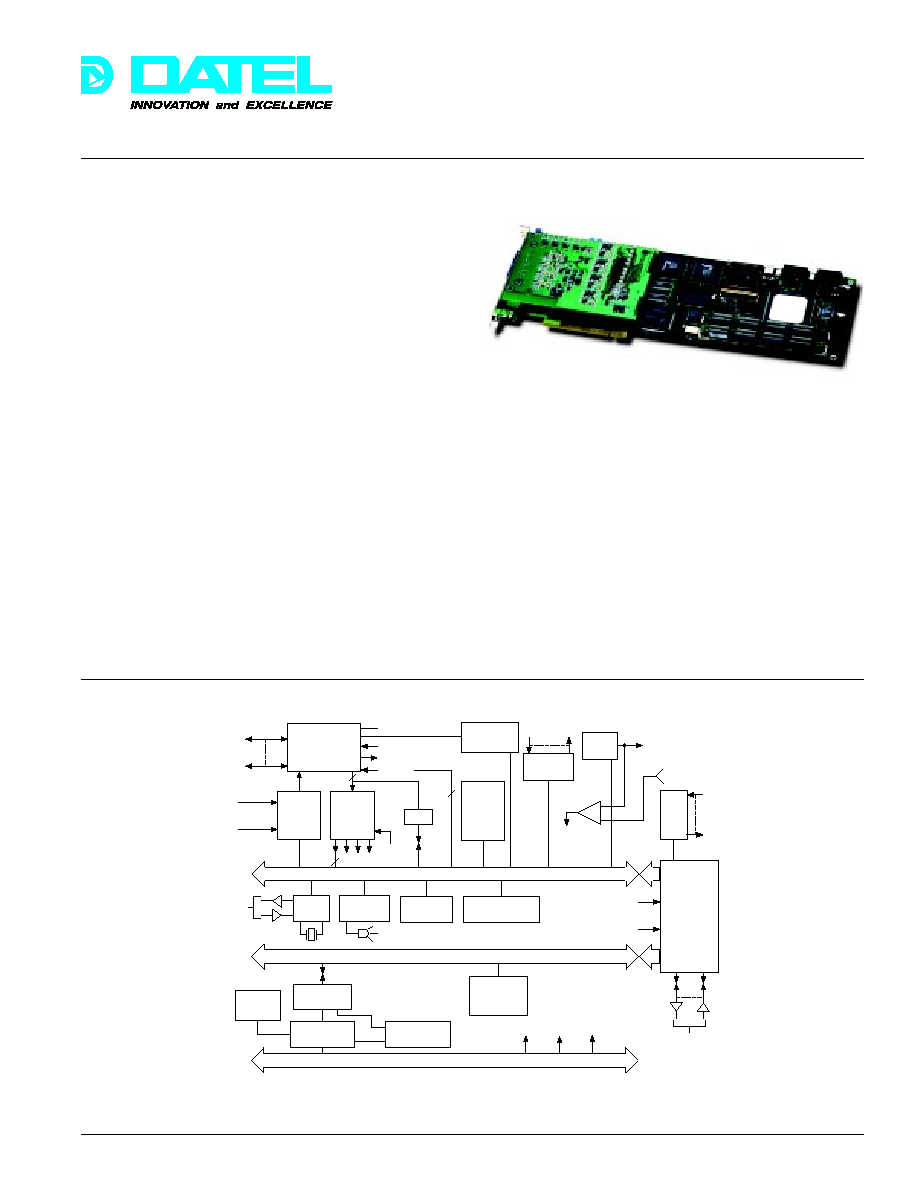
Figure 1. System Block Diagram
pluggable high-density "ADW" module, offering a choice of
input configurations. Current models include a four-channel
12-bit version, model PCI-431A, with up to 10MHz sampling
per channel. All four A/D converters sample at exactly the
same time. Model PCI-431C is similar with four 5MHz 14-bit
A/D's. Other models are planned.
The PCI-431's architecture offers true
multi-level concurrent
co-processing. Using a local First-In, First-Out (FIFO) A/D
memory and a bidirectional PCI bus FIFO, analog samples
may be stored
while DSP math continues while previous data
blocks are uploaded to the host PC.
Pluggable
A/D - D/A
Module Family
Freq
Synth/
Trig/
Timer
A/D
FIFO
Memory
4k x 32
Xcvr
SMT
SRAM
512k
x32
(2Mb)
E H F
RST
ISP/JTAG
2661
UART
DSP CMD
REG
DSP STAT
REG
Boot Flash
RAM 512k x 16
320C44
Digital
Signal
Processor
2-Way FIFO
and Mailbox
PCI Controller
S5933
512 x 32
x 2
32-Bit Global Bus
32-Bit Local Bus
PCI Bus
A/D Chan Addrs 0-4
A/D Model 0-3
Ctrl Bus
Bus
Expansion
Port
XDS-510
JTAG
Emulator
Port
Interrupts
Oscillator
4 COMM
Ports
+12V
+5V
-12V
All memory is shown at
maximum capacity.
RS-232-C
Serial I/O
External
A/D Clock
External
Trigger*
Analog
I/O
8
A/D Sample
Counter
D/A
Analog
Out
Analog
Trigger
Analog
Trigger
Serial
NVRAM
Pass-Thru
State Machine
LED
Lamp
SIMM SRAM
2 x 1M x 32
(8Mb)
32
32
DATEL, Inc., Mansfield, MA 02048 (USA)
∑
Tel: (508)339-3000, (800)233-2765 Fax: (508)339-6356
∑
Email: sales@datel.com
∑
Internet: www.datel.com
Æ
Æ
41

PCI-431
Æ
Æ
DATEL, Inc., Mansfield, MA 02048 (USA)
∑
Tel: (508)339-3000, (800)233-2765 Fax: (508)339-6356
∑
Email: sales@datel.com
∑
Internet: www.datel.com
This offers the most efficient division of tasks with the PCI-431
handling A/D sampling and signal math while the PC stores
data to disk and/or displays it on simultaneous screen
graphics.
A/D clocking may use an on-board programmable frequency
synthesizer, local crystal oscillator, or external clock input.
Frame triggering is either from an internal DSP timer or
analog or digital inputs. The analog trigger uses a threshold
comparator whose level is set by a programmable on-board
16-bit D/A converter. This D/A may also be used as a general
purpose analog output.
The 50MHz Texas Instruments 320C44 floating point zero-
wait-state Digital Signal Processor will execute two parallel
instructions in one CPU cycle and includes a wealth of high-
performance features such as on-chip Direct Memory Access
(DMA), numerous local interrupts, and programmable timers.
The DSP fully controls "Harvard architecture" dual 32-bit
busses and up to eight megabytes of high-speed on-board
static random access memory (SRAM). A flash boot RAM
stores initial code so the DSP automatically starts and waits
for download of additional code from the host, from the RS-
232-C serial port or via one of four on-board byte-wide COMM
ports. These COMM ports also extend the power of the
PCI-431 by connecting to nearby C40 DSP's on adjacent array
processors. Thus the PCI-431 may form the nucleus of a
powerful multiprocessor DSP system.
Data, code, and control/status from the PCI-431 passes
through the 512-word 32-bit BiFIFO which can read or be
written to from the PCI bus in burst bus master mode while
the DSP continues processing.
The combination of hardware design and software offers ring-
buffered pretriggering to collect data
before and after an
external event. A local programmable 24-bit sample counter
determines the frame length after each trigger for repeating
triggers or the number of samples after a pretrigger signal.
This exceptional design flexibility can collect single samples,
repeating samples, repeating frames of multiple samples, or
may sample "forever". The ring buffering can be confined only
Byte Address
Function
Directions
00300000-0037FFFFh
Flash Memory
Read/Write*
00380000-003D8000h
Local I/O Registers
See manual
00400000-0047FFFFh
Local SRAM
Read/Write
80000000h
Bidirectional FIFO Data Read/Write
80040000h
BiFIFO Mailbox
Read/Write
80080000h
Reset BiFIFO
Write
80100000-802FFFFFh
Global SIM SRAM
Read/Write
*Special prodecures are required to write to the Flash
memory.
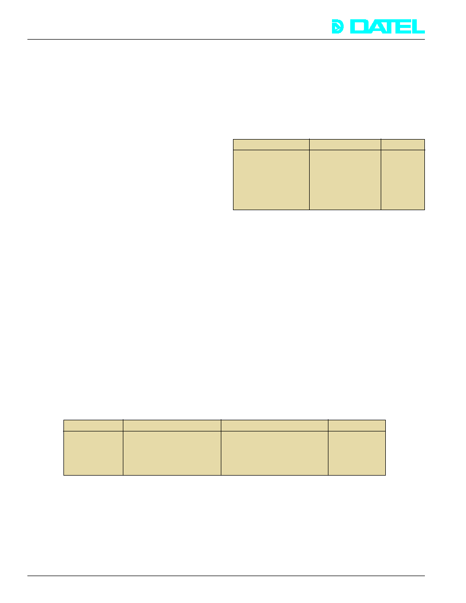
PCI-431 DSP Memory Summary
(Standard 320C44 memory reservations are not shown)
Command/Status
(Read/Write)
Phase Lock Loop Registers
(Write only)
A/D Sample Counter
(Write only)
A/D FIFO Data Register
(Read only)
Analog Module Select
(Read/Write)
Interrupt Control/Status Register
(Read/Write)
UART Serial Port Registers
(Read/Write)
Expansion Slot
(Rread/Write)
Generate PCI Interrupt
(Write only)*
Reset A/D FIFO
(Write only)
D/A Output Data Register
(Write only)
*Interrupts to PCI bus are fully maskable.
PCI-431 I/O Registers Mapped in Local DSP Memory
Region
Base Address Register
Function
Direction
Not Applicable
BADR0
S5933 Operation Registers
Read/Write
Region 0
BADR1
Reserved
Region 1
BADR2
BiFIFO Mailboxes
Read/Write
Region 2
BADR3
BiFIFO Data
Read/Write
Region 3
BADR4
BiFIFO Reset
Write
PCI Pass-Thru Regions
to the PCI-431's fast on-board memory or can use available
memory on the host PC for very large buffers. The bus
master controller may temporarily take control of the PCI bus
and burst arrays directly to PCI memory in DMA mode. The
design is fully streaming and will not lose samples while filling
host memory or disk of hundreds of megabytes.
42

PCI-431
Æ
Æ
DATEL, Inc., Mansfield, MA 02048 (USA)
∑
Tel: (508)339-3000, (800)233-2765 Fax: (508)339-6356
∑
Email: sales@datel.com
∑
Internet: www.datel.com
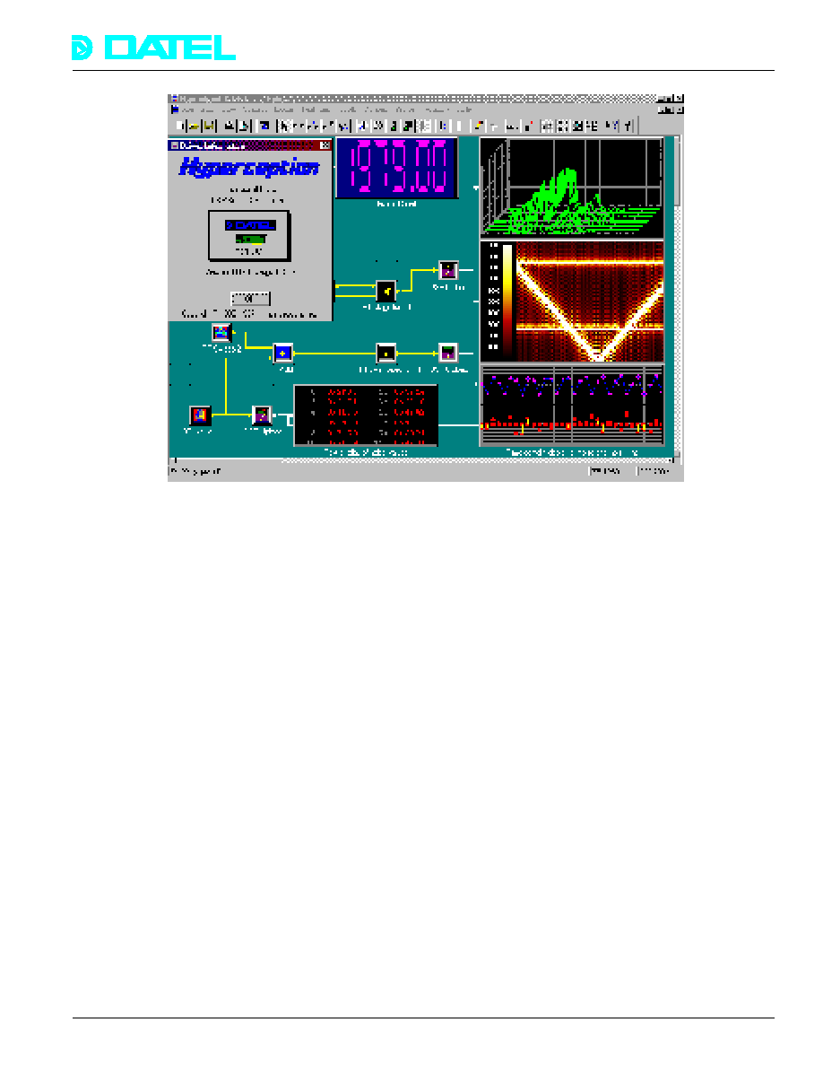
Figure 2. Hyperception RIDE Block Diagram Worksheet
Hyperception RIDE
The Hyperception Real Time Integrated Development
Environment (RIDE) for DSP offers connect-the-boxes graphic
"block diagram" control of the PCI-431 without having to learn
DSP programming. RIDE operates under Windows 95 or
Windows NT and includes a comprehensive library of several
hundred DSP, math, array matrix, I/O, and data processing
functions all selected by movable screen icons on a
worksheet. These functional blocks cover
both the local DSP
operation
and activity on the host PC. Once the diagram is
designed, the system "compiles" it to high-speed binary code,
downloads it to the PCI-431 and collects data to screen, host
buffer, disk, or other destination. The user may graphically
"single step" the operation and debug the application "live".
Sections of the block diagram worksheet may be saved to a
library as functional modules described by a single icon.
Thus, debugged modules are available for multiple user
applications. RIDE will operate concurrently with other boards
and processes in the system.
With RIDE for the PCI-431, the user does not have to learn a
computer language but may integrate his or her own software
functions if desired. Related Hyperception products will
generate "C" source code from the block diagram graphics or
a complete preprogrammed executable file (the "HAPPI"
system) for non-technical operators. Hyperception also offers
fully compatible image processing and communications
products for the PCI-431.
DATEL AFB System
DATEL's Application Function Block (AFB) System (model
PCI-431WIN) is a simple, easy-to-learn, PCI-431 command
sequencer running under Windows 95 or NT. The system
initializes all hardware, starts the A/D, saves data to disk and
plays back screen graphics. The AFB system also includes a
real-time "oscilloscope" screen mode and a hex DC calibration
utility. It will run numerous DSP functions at high speed
(including FFT's) and exercises all hardware on the board. A
small DSP library is included, and the AFB system is sufficient
to perform many applications.
AFB operation is defined by function blocks under Windows 95
which invoke tokens. The user selects these tokens after
designing the application. The list of tokens correspond
directly to internal functions previously downloaded to the
PCI-431. The assembled token stream is then downloaded to
the DSP where it is processed in sequence and executed.
Simple nested loops are supported.
Data is passed as files to the host PC where further file
processing may use any spreadsheet or data base program or
a simple user program. The AFB system serves as an
example of how to program the PCI-431 and includes many
low level functions to extract for integration with your code. Or
you may add your own functions to the DATEL AFB library.
43

PCI-431
Æ
Æ
DATEL, Inc., Mansfield, MA 02048 (USA)
∑
Tel: (508)339-3000, (800)233-2765 Fax: (508)339-6356
∑
Email: sales@datel.com
∑
Internet: www.datel.com
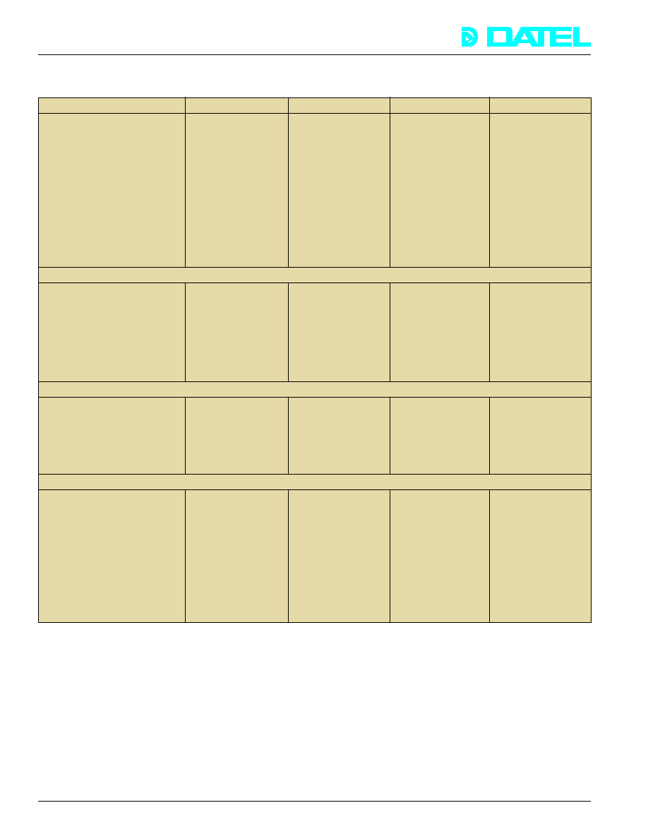
FUNCTIONAL SPECIFICATIONS
(Typical at +25∞C, dynamic conditions, gain = 1, unless noted)
ANALOG INPUTS
Number of Channels
Input Configuration
Analog Module Type
Full Scale Input Ranges
[Note 3]
Input Overvoltage
[Note 2]
(sustained, no damage)
Input Impedance
Channel Addressing
Modes
[Note 7]
Input Connector
Number of A/D's
Resolution
Conversion Time
[Note 12]
Unipolar Output Coding
[Note 8]
Bipolar Output Coding
[Note 8]
Integral Non-linearity
Differential Non-linearity
Gain Error
Offset/Zero Error
Full Scale Tempco
Offset/Zero Tempco
Sampling Rate
(single channel) [Note 12]
Sampling Rate to FIFO
(all channels simultaneous)
[Note 6]
Sampling Rate to DSP Memory
(all channels simultaneous)
[Note 6]
Total Harmonic Distortion
Full Power Input Bandwidth
[Note 11]
PCI-431A
4 non-isolated
Single-ended
[Note 1]
ADW-12A
±2.5V or 0 to +5V
(user selectable)
±12V
1 kilohm
Two or four
channels, simul.
25-pin "D"
Four
12 bits
100 ns max.
Straight binary
Offset binary or two's
complement
±2 LSB
±1 LSB
Adj. to zero
Adj. to zero
±0.2 LSB/∞C
±0.1 LSB/∞C
1 kHz min.,
10 MHz max.
10 MHz per chan.
5 MHz per chan.
≠72 dB [Note 4]
10 MHz
PCI-431B
2 non-isolated
Single-ended
[Note 1]
ADW-12B
±2.5V
±12V
500
or 50
One or two
channels, simul.
SMA Coaxial
Two
12 bits
25 ns max.
--
Two's complement
±2 LSB
±1.5 LSB
6.5%
Adj. to zero
±1 LSB/∞C
≠2 LSB/∞C
5 MHz min.,
40 MHz max.
40 MHz per chan.
10 MHz per chan.
≠62 dB [Note 22]
40 MHz
PCI-431C
4 non-isolated
Single-ended
[Note 1]
ADW-14C
±2.5V or 0 to +5V
(user selectable)
±12V
1 kilohm
Two or four
channels simul.
25-pin "D"
Four
14 bits
333 ns max.
Straight binary
Offset binary or
two's complement
±3 LSB
±2 LSB
Adj. to zero
Adj. to zero
±0.2 LSB/∞C
±0.1 LSB/∞C
1 kHz min.,
3 MHz max.
3 MHz per chan.
3 MHz per chan.
≠82 dB [Note 5]
10 MHz
PCI-431D
16 non-isolated
Single-ended
[Note 1]
ADW-14D
±2.5V
±12V
1 µA leakage
2 to 16 channels
simul. [Note 16]
25-pin "D"
Sixteen
14 bits
2.2 µs
--
Two's complement
±3 LSB
±2 LSB
[Note 18]
[Note 18]
[Note 18]
[Note 18]
370 kHz max.
300 kHz per chan.
300 kHz per chan.
≠82 dB
15 MHz
SYSTEM DYNAMIC PERFORMANCE
SYSTEM DC CHARACTERISTICS
[Note 6]
A/D CONVERTER
44

PCI-431
Æ
Æ
DATEL, Inc., Mansfield, MA 02048 (USA)
∑
Tel: (508)339-3000, (800)233-2765 Fax: (508)339-6356
∑
Email: sales@datel.com
∑
Internet: www.datel.com
FUNCTIONAL SPECIFICATIONS
(Typical at +25∞C, dynamic conditions, gain = 1, unless noted)
ANALOG INPUTS
Number of Channels
Input Configuration
Analog Module Type
Full Scale Input Ranges
[Note 3]
Input Overvoltage
(sustained, no damage)
Input Impedance
Channel Addressing
Modes
[Note 7]
Input Connector
Number of A/D's
Resolution
Conversion Time
[Note 12]
Unipolar Output Coding
[Note 8]
Bipolar Output Coding
[Note 8]
Integral Non-linearity
Differential Non-linearity
Gain Error
Offset/Zero Error
Full Scale Tempco
Offset/Zero Tempco
Sampling Rate
(single channel) [Note 12]
Sampling Rate to FIFO
(all channels simultaneous)
[Note 6]
Sampling Rate to DSP Memory
(all channels simultaneous)
[Note 6]
Total Harmonic Distortion
Full Power Input Bandwidth
[Note 11]
PCI-431E
4 non-isolated [Note 1]
Differential
[Note 19]
ADW-16E
±2.5V
±12V
1 kilohm
Two or four
channels, simul.
Subminiature "D"
Four
16 bits
2.8 µs max.
--
Two's complement
±5 LSB
±2 LSB
Electronic trim
Electronic trim
±3 LSB/∞C
±0.1 LSB/∞C
333 kHz max.
268 kHz
268 kHz
≠91 dB
5 MHz
PCI-431L
16 non-isolated
Single-ended
[Note 1]
ADW-12L-1 or -2
±2.5V or 0 - +4.096V
(two models)
±1 µA leakage
[Note 2]
2 to 16 channels,
simul. [Note 16]
25-pin "D"
Sixteen
12 bits
650 ns
--
Straight binary,
offset binary
±2 LSB
±1 LSB
[Note 20]
[Note 20]
[Note 20]
[Note 20]
1 MHz
600 kHz
600 kHz
≠79 dB
20 MHz
SYSTEM DYNAMIC PERFORMANCE
SYSTEM DC CHARACTERISTICS
[Note 6]
A/D CONVERTER
45
PCI-431F
4 non-isolated
Single-ended
[Note 1]
ADW-14F
±2.5V or 0 - 5V
±12V
1 kilohm
2 or 4 channels,
simul.
25-pin "D"
Four
14 bits
100 ns
--
Straight bin., offset
bin., two's comp.
±3 LSB
±2 LSB
Adj. to zero
Adj. to zero
±0.5 LSB/∞C
±0.2 LSB/∞C
1kHz min.,
10 MHz max.
10 MHz per channel
5 MHz per channel
≠75 dB
10 MHz

PCI-431
Æ
Æ
DATEL, Inc., Mansfield, MA 02048 (USA)
∑
Tel: (508)339-3000, (800)233-2765 Fax: (508)339-6356
∑
Email: sales@datel.com
∑
Internet: www.datel.com
SPECIFICATIONS, CONTINUED
(Typical @ +25∞C, dynamic conditions, unless noted)
A/D CLOCK, TRIGGER, AND SAMPLE COUNTER
A/D Sample Clock Sources
1. 20-40 MHz frequency
[Note 13]
synthesizer
2. Synthesizer divider (any
integer 2 - 65536)
3. Fixed 10, 25, or 50 MHz CPU
clock
4. CPU clock divided by any
integer 2 - 65536
5. External (user supplied) clock
on P3 internal header (TTL levels)
6. On-board crystal oscillator
(user installable)
Trigger Input
TTL logic levels, edge triggered.
Triggering occurs on the falling edge.
Trigger Function
Each trigger starts a frame with a
programmable number of A/D samples
per frame.
Trigger Sources
Selectable between TCKL0 timer from
[Note 14]
DSP, external digital trigger input,
pretrigger mode, or external analog
trigger.
Response to Trigger
Selectable from among:
1. A trigger starts one frame of
A/D samples ("single trigger").
2. Starts repeating frames of
samples, each started by an
internal trigger ("continuous
trigger").
3. Runs the A/D "forever" with the
sample counter disabled.
Sampling is terminated by
counting frames.
4. Pretrigger mode (see below).
Internal Trigger Range
25 MHz (CPU clock/2) divided by 1 to
2^32 (40ns to 12.2 hours).
Generated by DSP TCKL0
External Analog Trigger
Uses the on-board D/A channel and a
comparator to start a frame. Allow a
2µs delay after threshold crossing.
Triggering occurs on the rising slope.
Analog Trigger Input Range
±10V
Analog Trigger Hysteresis
±40 mV
A/D Samples per Frame
1 to 16,777,216 samples. Load one
less than the desired sample count
and do not load less than 2. The
sample counter may be disabled for
frames longer than 16 million.
Pretrigger Mode
A/D sampling begins with an internal
trigger. The sample down-counter is
delayed until an external trigger.
Sampling stops when the sample
count is reached. Data is stored in a
ring buffer for analysis before and
after the external trigger.
LOCAL DSP MICROCOMPUTER
CPU Type
One Texas Instruments floating point
320C44, 50 MHz
Local Data Busses
Local, 32 bits. Global, 32 bits.
Flash Boot Memory
Up to 512k x 16 bits (standard is
128k x 16)
On-board Local Memory
Up to 512k x 32 bits surface mount
SRAM (2M b). Standard is 128k x 32.
On-board Global Memory
Up to 2 x 1M x 32 bits SIMM
SRAM (8 Mb). Standard is 2 x 256k
x 32 (2 Mb).
Local DMA Controller
Internal to DSP
Local Interrupts to DSP
Bidirectional output FIFO is empty,
A/D sample count reached, A/D FIFO
half full, bidirectional input FIFO has
data. NMI - connected to COMM
ports.
COMM Ports
Four byte-wide DSP COMM ports,
approx. 14 MHz max. rate. Uses four
internal 30-pin header connectors.
JTAG/ISP Port
For programming and verification of
internal logic devices (internal header,
P5, 8 pins).
Emulator Port
Internal header P11, 14 pins.
Compatible to XDS510 emulator.
DSP Reset
DSP reset may occur from PCI bus
reset bit, on-board reset pushbutton,
software reset instruction, power-on
reset, or COMM port reset.
Serial Port
On-board 2661 UART and RS-232-C
transcievers for diagnostics, local
monitor, etc. Programmable data
length, stop bits, synch/asynch and
baud rate (max.115 kilobaud). I/O is
on an internal 10-pin header.
DSP Expansion Slot
Contains a subset of the local bus,
32-bit data, 8-bit address. The port is
selected at DSP address 003B8000.
CAUTION - This port is unbuffered.
A/D Memory
4096 x 32 bits First-In, First-Out,
includes empty, half full and latched
full signals.
Data Bus Size
32 bits
Address Bus Size
32 bits
Data Transfer
32-bit I/O or memory (selectable)
PCI Controller
AMCC S5933, bus master or slave
mode
Interrupt to PCI Bus
Controlled by on-board DSP software.
Selectable INTA#, INTB#, INTC#, or
INTD# to PCI bus.
Bidirectional FIFO
2 x 512 x 32 bits dual bidirectional
(BiFIFO) [Note 15]
FIFO between PCI controller and DSP
global bus. Includes control/status
mailbox and interrupt.
PCI BUS INTERFACE
46

PCI-431
Æ
Æ
DATEL, Inc., Mansfield, MA 02048 (USA)
∑
Tel: (508)339-3000, (800)233-2765 Fax: (508)339-6356
∑
Email: sales@datel.com
∑
Internet: www.datel.com
ANALOG OUTPUT
Number of Channels
One channel mounted on DSP carrier
board.
Functions
Selectable as general-purpose analog
output or analog trigger comparator
threshold reference.
Resolution
16 bits
Output Voltage Range
≠10V to +10V at 5 mA max.
Linearity
±0.01% of FSR
Settling Time
10 µs (10V step)
Input Coding
2's complement
D/A Connector
P3 10-pin internal header (shared
with other functions).
Analog Module PCB
Outline Dimensions
5" L x 3.313" W
Analog Module Bussing
Besides many A/D controls, the ADW
includes an 8-bit write-only control bus
and bidirectional read/write 32-bit data bus.
LED Lamp
Internal green light-emitting diode
lamp programmable by the user for
diagnostics, etc. Visible only when
the computer cover is removed.
System Warmup Time
15 minutes to achieve rated accuracy.
[Note 9]
Board Identification
Internal 4-bit solder gap is factory
Code
preset to identify analog module type.
May be changed if another module is
present
Operating Temp. Range
0 to +60∞C. Forced cooling is required.
No thermal shock.
Storage Temp. Range
≠25 to +85∞C
Relative Humidity
10% to 95%, no condensation
Altitude
0 to 10,000 feet
Power Required
+5V at 1.5A typ., 2A max.
from PCI Bus
±12V at 200 mA typ. , 250 mA max.
use +3.3V power.
PCB Outline Dimensions
4.187" W x 12.313" L x 0.75" H (SIMM
[Note 10]
height above PCB)
Number of Slots
One slot [Note 10]
Bootstrap Flash Code
The DSP automatically loads and
runs from the flash. After
initialization, it attempts to run a
COFF file downloaded through the
BiFIFO.
Fabrication
Double-sided, high density, multi-layer
surface mount. CAUTION - Do not
flex the board or apply mechanical
stress.
4.
PCI-431A test conditions: 1 MHz filtered sinewave input, amplitude = full
scale ≠0.5 dB. THD uses the first six harmonics.
5.
PCI-431C test conditions: 500 kHz filtered sinewave input, amplitude = full
scale -0.5 dB. THD uses the first six harmonics.
6.
The aggregate total sample rate to the A/D FIFO memory is
(NumberChannels) x (MaxSampleRatePerChannel).
7.
Models PCI-431A -431C, and -431F always transfer either two samples or
four samples simultaneously sampled with each A/D clock. Data transfers
are always 32 bits wide with A/D samples right justified within each 16-bit
word. The SSH control bit selects whether two or four channels are collected
together. The channel address automatically wraps around to zero after
collecting the highest channel. Model PCI-431B transfers two single channel
samples
separately clocked but packed into a 32 bit dword.
8.
Output data is right justified without sign extension. For multiple channels,
data is loaded to the A/D FIFO memory sequentially multiplexed by channel
address. For example, with 4-channel inputs, the output channel sequence
is 0, 1, 2, 3, 0, . . .
9.
The system must be allowed to stabilize after high thermal gradient or
thermal shock conditions.
10. A PCI board mounted in the slot adjacent to the PCI-431 (component side)
should be 7.25 inches maximum depth from the back mounting plate. Adjacent
boards longer than this will fit but should use a non-conductive plastic or
cardboard separator. The PCI-431 is over 12 inches long. Make sure there is
no interference from fans, disk drives, brackets, or adjacent hardware.
11. Full power input bandwidth is that sinusoidal input frequency for which the
equivalent amplitude of the quantized digital output is ≠3 dB from that at low
frequencies. Since this input frequency is generally "beyond Nyquist", it is useful
only if the aliasing effects are fully understood. The input sinewave must be well
filtered and achieve harmonic distortion less than ≠96 dB. Note that this input
specification implies that some level of output attenuation may begin within the
Nyquist sampling rates (input spectra <0.5 the maximum sampling rate).
12. There is a hierarchy of available speed from the A/D converters. The times
shown are the fastest hardware throughput from a single A/D channel into
the on-board A/D FIFO memory. Transfers to local DSP memory may take
somewhat longer depending on concurrent DSP processing. Bus master
block transfers to PCI bus depend on many system factors plus the on-going
DSP processing and must be tested for each system.
13. The user may install a crystal and driver "can" oscillator for the A/D clock.
This allows the user to have an oscillator as stable and accurate as needed.
14. If external triggers are used with internal A/D sample clocking, samples will
be collected at the next A/D clock after the trigger.
15. The Bidirectional FIFO is transparently cascaded through the S5933
controller FIFO in PCI bus master mode.
16. Channel Addressing Modes: Models PCI-431A, C, D, E, F, and L will sample
all of their channels simultaneously or can be short-cycle addressed,
transferring fewer channels than their full capacity. Short-cycling always
transfers an even number of channels starting at channel zero (0-1, 0-3,
etc.). Short-cycle addressing is controlled by the Channel Address Register
on the DSP carrier board.
17. Models A, B, C, and F use pipelined A/D converters with some sample clock
delay between the start of conversion and output data ready.
18. The PCI-431D uses pre-trimmed A/D converters. The offset error over the
full temperature range is ±5 LSB (typ.) and the gain error is ±20 LSB (typ.)
over the temperature range.
19. The PCI-431E Common Mode Input Range is ±2.5V and the Common Mode
Rejection is 60 dB, DC to 60 Hz.
20. The PCI-431L uses pre-trimmed A/D converters. The offset error over the
full temperature range is ±6 LSB (typ.) and the gain error is ±15 LSB (typ.)
over the temperature range.
21. Models PCI-431D, E, and L employ a switched-capacitor input to each A/D
converter. This type of input reflects minute amounts of charge back to the
external input circuit. Also the effective input capacitance changes at the A/D
sampling rate. Normally these conditions are of no consequence to driving
sources under 1000 ohms. If necessary, consider using a stable, fast-
settling amplifier on each input.
22. PCI-431B test conditions: 9.68 MHz filtered sinewave input. Amplitude = FS
≠ 0.5 dB, external 40 MHz clock. The THD uses the first six harmonics.
MISCELLANEOUS
FOOTNOTES
1.
The simultaneous sampling single-ended models may operate in "software
differential" mode by connecting two single-ended A/D's to each external
differential input channel. Then subtract the resultant data in software after
A/D conversions are done.
2.
For models with 50
input impedance sustained overvoltage is ±5V and
momentary overvoltage is ±12V.
3.
The standard configuration is bipolar inputs (where available) and offset binary
coding unless noted. Input ranges and output coding are changed by modifying
jumpers or solder gaps on the analog module. Or some versions require
separate models and cannot be converted between unipolar and bipolar.
47

PCI-431
Æ
Æ
DATEL, Inc., Mansfield, MA 02048 (USA)
∑
Tel: (508)339-3000, (800)233-2765 Fax: (508)339-6356
∑
Email: sales@datel.com
∑
Internet: www.datel.com
A/D Data Format
A/D data is delivered as a stream from the FIFO memory.
For multichannel inputs, this means that data is multiplexed by
the channel address with a modulo address wrap-around at
the top channel. For example, with 4-channel inputs, the
output channel sequence is 0, 1, 2, 3, 0, 1, . . . One additional
factor is that the 32-bit wide dual FIFO contains two A/D
samples. Therefore the longword sequence is 0,1 . . . 2,3 . . .
0,1 . . .
The FIFO output can take two formats depending on which
analog module is used and whether single-channel or
autosequential (autoincrement) channel addressing is
selected. For single-channel mode, data appears as follows:
31 16
15 0
Sample N+1
Sample N
If the addressing is selected for autoincrement, data appears
this way:
31 16
15 0
Channel N+1 Channel N
Note that all A/D data is right-justified within the 16-bit data
word with upper bits beyond the A/D resolution going unused.
Models PCI-431A and 431C always transfer either two
samples or four samples simultaneously sampled with each
A/D clock. Data transfers are always 32 bits wide with A/D
samples right justified within each 16-bit word. The SSH
control bit selects whether two or four channels are collected
together. The channel address automatically wraps around to
zero after collecting the highest channel. Model PCI-431B
transfers two samples
separately clocked but packed into a 32
bit dword.
Trigger and Sample Count Systems
The PCI-431 accepts one of three triggers - external analog,
internal, or external digital. All three initiate identical internal
actions. For the internally generated trigger, either a single
trigger can be accepted ("single trigger mode") or the trigger
can repeat ("continuous trigger mode") with programmable
delays between each trigger.
The trigger starts a frame of samples. Each frame can be
from one to 16,777,216 samples using the 24-bit counter. The
system will collect the number of samples in the sample
counter then stop and wait for the next trigger. Meanwhile,
the sample counter will automatically reload in anticipation of
the next trigger. Data flows into the FIFO memory which will
notify the DSP that it has data to be saved. The FIFO size is
independent of the frame size, therefore FIFO flags will occur
independently from the sample counter.
A DSP interrupt can be generated after each frame completes
or at each FIFO half full signal.
The PCI-431 will automatically control its own channel
addressing such that the address advances immediately as a
sample is sent to the FIFO. In single-channel mode, each
frame will consist of data from only the selected channel. In
automatic sequential addressing ("autoincrement"), the frame
will contain one or more scans of channels, with addresses
automatically wrapping around according to the channel
capacity of the analog module.
The combination of programmable sample count, frame rate,
A/D rate, and channel addressing mean that practically all
conceivable applications can be accomplished. The basic
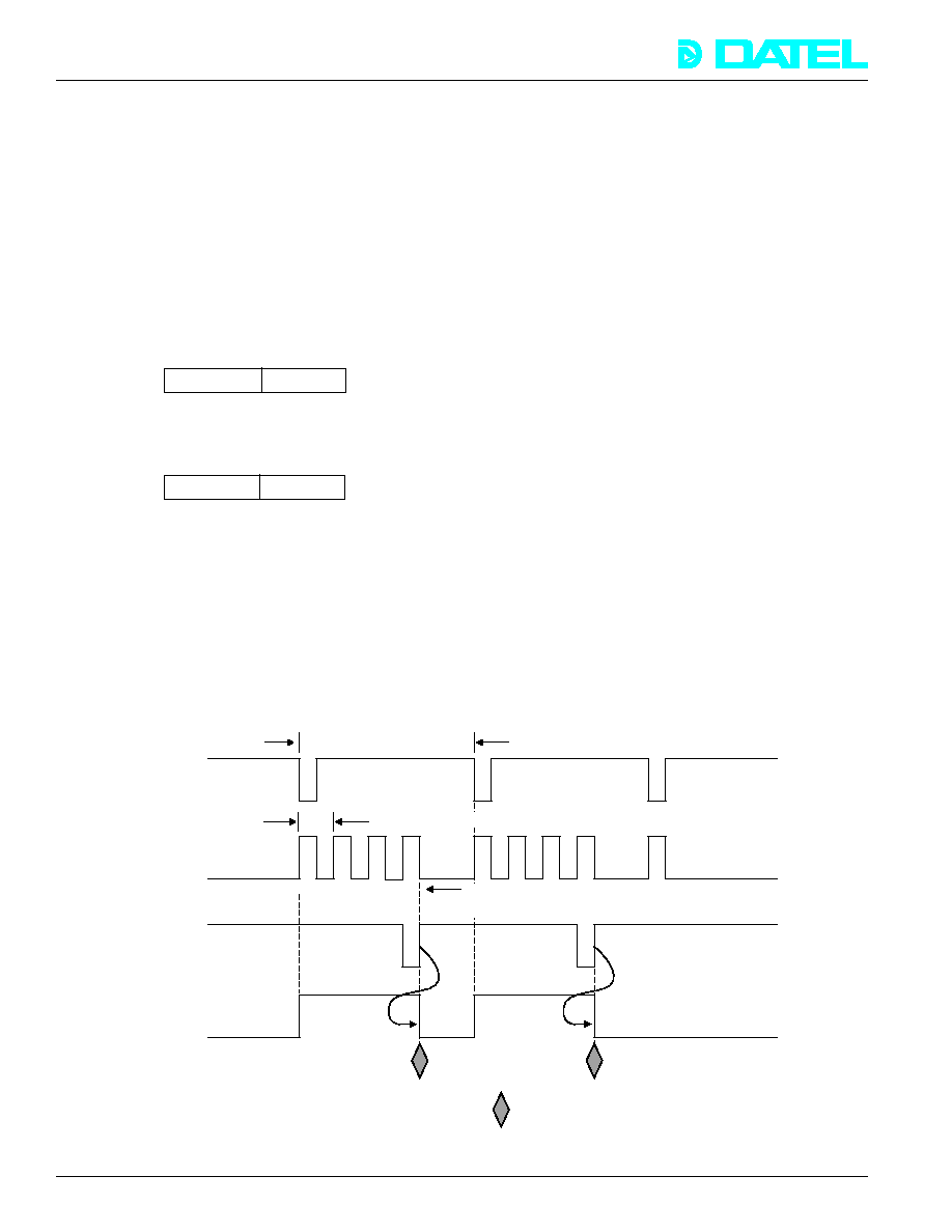
system timing is shown in Figure 3.
Figure 3. PCI-431 A/D Timing Diagram
Internal or external trigger rate
TRIGGER*
A/D
START
CONVERT
END OF
SCAN*
(Internal
signal)
ACQUIRE
FLAG
0
1
2
3
Internal or external start rate
Fixed or sequential channel addressing up to
16M samples per trigger
Maskable Interrupt and Status
48

PCI-431
Æ
Æ
DATEL, Inc., Mansfield, MA 02048 (USA)
∑
Tel: (508)339-3000, (800)233-2765 Fax: (508)339-6356
∑
Email: sales@datel.com
∑
Internet: www.datel.com
Pre/Post Trigger Transient Capture Applications
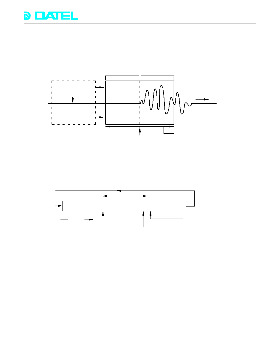
A certain class of applications requires data sampled relative to one or more external events. Data before and after the event
need to be analyzed. If the exact time of those external events cannot be predicted accurately but the event can be identified
with a trigger, data must be recorded continuously then processed after the event occurred. At higher sample rates, the user
must use all memory storage, which has limited capacity, but is still large enough to capture the event. A ring buffer circular
storage method is used in which new samples continually overwrite the oldest samples.
Figure 4. Transient Signal Capture
The PCI-431 accepts either a digital or analog (threshold trip) event trigger. An on-board D/A converter sets the comparator
voltage level for the analog trigger. The system stores data before and after the trigger. A post trigger sample counter selects
the number of offset samples after the trigger. The number of pretrigger samples equals the total circular storage minus the post
trigger size. Note that pretrigger samples in Figure 5 are skewed over the buffer tail.
Figure 5. A/D Data Ring Buffering
A/D collection continues after the trigger until the system has stored the number of samples specified in the sample counter. The
trigger sample can be found using backwards circular offset from the last sample saved. Multiple external events can be
identified using a combination of the post trigger method and the marker inputs.
The PCI-431 can access huge PCI memory. Collected A/D samples can then be saved to disk or tape.
System Throughput
All specifications listed here describe performance available on the
board. Actual transfer rates out to system memory, disk,
network, or other data destinations depend on many other factors. These include the memory type and memory controller, host
software Operating System, disk interface, number of disk drives, buffer sizes, type of disk controller, number and method of
simultaneous applications, DMA usage, CPU type and speed, bus loading, software design, etc. It is not practical to state a
single set of performance specifications for the total
system, however, DATEL can give you guidelines for a specific configuration.
For speed-critical applications, the full system must be thoroughly tested to develop actual performance.
Analog Input
Signal
Sliding Window
Trigger
Total Circular Buffer Length
Time
Post Trigger
Pretrigger
Head
Tail
Pretrig Samples
Posttrig Samples
Pretrig Samples
Trigger
Oldest Sample
Last Sample Collected
"Offset"
Sample Count
49

PCI-431
Æ
Æ
DATEL, Inc., Mansfield, MA 02048 (USA)
∑
Tel: (508)339-3000, (800)233-2765 Fax: (508)339-6356
∑
Email: sales@datel.com
∑
Internet: www.datel.com
RIDE Function List
The following is a
partial list of standard functions included
with Hypersignal
Æ
RIDE. Functions listed with an asterisk (*)
are included in RIDE Lite.
Arithmetic Functions
*Absolute Value, *Add, Complex Conjugate, *Complex to Real,
dBAmplitude, dBPower, *Differentiate, *Divide, *Exponential,
Four or Five Input Add, *Integrate, *Log, *Log 10, *Logx(y),
*Modulo, *Multiply, Polar to Rectangular, *Power, Product,
*Real to Complex, *Reciprocal, Rectangular to Polar, *Square,
*Square Root, *Subtract, *Sum, Three Input Add
Bit Conversion Functions
Bit Mask, *Ones Complement, Pack, *Shift Left, *Shift Right,
Unpack
Communications Functions
1st Order Butterworth Filter, *Automatic Gain Control,
Averaged Periodogram, Bit Error Rate, *Fixed Offset, *Gain,
Integrate and Dump, Leaky LMS Adaptive Filter, Least Mean
Square Adaptive Filter, First Order Loop Filter, Numerically
Controlled Oscillator, Periodogram, Phase Decoder, Phase
Locked Loop, PSK (Phase Modulation), *Rectify, *Spectral
Inversion, Strobe
Companding
µ-255 Decode/Encode, A-87.6 Decode/Encode (A law)
Conditional Operators
Equal, Greater Than, Greater Than/Equal, Less Than, Less
Than/Equal, Loop Counter, NOT, Not Equal
Digital Logic Functions
*1 to N Demultiplexer, *N to 1 Multiplexer
Displays
*2-Channel Display, *Digital Display, *Single Channel Display,
*Text Display, *XY Display
DSP Functions
1/3 Octave Band Analyzer, 2-Sided Magnitude or Phase,
*Accumulate, *Autocorrelation, Biquad, *Center Clip, *Clip,
*Convolution, *Correlation, Dead Band, *Decimate, *FIR Filter,
Frame Accumulate, Frame Peak Position, *IIR Filter, *Interpo-
late, *Magnitude, *Median Filter, Octave Band Analyzer,
*Offset, *Phase, *Power Spectrum, Quantizer, Scale, *Thresh-
old, Transfer Function, *Zero Crossing
File I/O Functions
*File Read/Write, Multi File Read, * Super File Read
Frame Functions
*Buffer, *Concatenate, *Extract Sample, *Frame Count,
*Frame Information, Frame Shift, Frame Size, Framesize
Conversion, Overlap Buffer, *Pad, Peak Hold, *Replace
Sample, *Reverse, Rotate, Search, Sort, *Split, *Subset
General Functions
*Convert (float-integer-float), *Delay, Recursion, Sample-and-
Hold, Table Lookup, *Terminate Block Diagram
Logical Functions
4 Input AND, 4 Input OR, Decimal to Binary, *Logical AND,
NAND, NOR, NOT, OR, XOR
Multi Channel
*Interleave or Separate N Channels
Signal Generators
Complex Exponential, *Constant Generator, *Cosine Genera-
tor, Gaussian Generator, Impulse Generator, Noise Genera-
tor, PRN Generator, Pulse Train, *Ramp Generator, *Sine
Generator, *Square Wave Generator, *Sweep Generator,
*Triangle Wave Generator
Speech Functions
Adaptive Differential Pulse Code Modulation Decoder or
Encoder, Linear Predictive Coding
Statistical Functions
4 Input Max, Covariance, Event Counter, Exponential Fit,
Frame Cumulative, *Frame Maximum, *Frame, Mean, *Frame
Minimum, *Frame Range, *Frame Standard Deviation, Global
Cumulative, Global Frame Mean, *Global Maximum, *Global
Mean, *Global Minimum, *Global Range, *Global Standard
Deviation, *Global Variance, Histogram, *Linear Fit, Polyno-
mial Fit, *Root Mean Square
Transforms
Cepstrum, Chirp Z-Transform, Complex Cepstrum, DCT,
*DFT, Fast Hartley Transform, *FFT, Four Freq. Goertzel
Algorithm, *Frequency Zoom, Goertzel Algorithm, Hilbert
Transform, Inverse DCT, *Inverse DFT, Inverse Fast Hartley
Transform, *Inverse FFT, Inverse Hilbert Transform
Trigonometric Functions
*ArcCosine (x), *ArcSine (x), *ArcTangent (x), *Cosine(X),
*Hyperbolic Cos(x)/Sin(x)/Tan(x), *Sinc(x), *Sine(x),
*Tangent(x)
User Controls
Analog Meter, Data Display, Fader, Function Generator,
Keypad, Knob, LED Meter
Wave I/O Functions
*Wave Player/Recorder
Wavelet Functions
Daub4 or 6 Discrete Wavelet Transform with 4 or 6
Daubechies Coefficients
Window Functions
*Bartlett Window, *Blackman, *Boxcar, Gaussian, *Hamming,
*Hanning, Kaiser, Saramaki, Welch
50

PCI-431
Æ
Æ
DATEL, Inc., Mansfield, MA 02048 (USA)
∑
Tel: (508)339-3000, (800)233-2765 Fax: (508)339-6356
∑
Email: sales@datel.com
∑
Internet: www.datel.com
Application Function Block System
The AFB system was designed to satisfy several competing
objectives:
∑ It is easy to learn and use.
∑ It does not require DSP programming (but you must
understand your application).
∑ It can be modified, customized and expanded by adding
your own code.
∑ The system is reasonably powerful because of numerous
library modules.
∑ AFB's offer high performance and achieve most of the
speed of the DSP.
∑ Exercise the board hardware to verify that it is operational.
∑ The whole system is open so that developers can fully
understand it and adapt it to specific applications.
Combined with the host-side Commander interface, the AFB
system will do three simultaneous tasks at high speed without
sample loss:
∑ Super-fast, high-data-quality, non-stop streaming A/D
sampling
∑ Concurrent DSP math operations
∑ Swapped buffer uploads to the host PCI computer
The AFB system consists of a library of functions to control the
PCI-431, a command list processor (the "Scheduler" on the
DSP) and a host side interface system (the "Commander").
The DSP portion of the system is downloaded at start up as a
large COFF binary file from the PCI host to DSP memory (or is
"cross-loaded" from the NVRAM).
To operate the PCI-431, the user builds an AFB text source
file and passes this to the Commander to process. The
Commander converts this to a stream of 32-bit binary tokens
which are copied one time to the Scheduler running on the
DSP. This token control list remains resident in DSP memory
all during the time the AFB system is active. The DSP
Scheduler then calls specific AFB functions which were
previously downloaded within the Scheduler's function library.
The tokens are called one after another as fast as possible
and the operation sequence exactly follows that built in the
user's AFB source file. In fact, each called AFB function
consists of a "C" or assembly module using a special
parameter passing method.
The AFB system supports simple nested loops for hierarchical
control. It uses a sophisticated double swapped buffer system
(both input and output swapped buffer pairs) to retain high
speed and no lost data. While it is not a full computer
language (there are no address labels, returned values,
conditional branching, etc.), these operations are easily added
by inserting your own "C" or assembly code and rebuilding the
AFB system.
The Commander now assumes a data processing role once
the initial AFB download and start occurs. As the Scheduler
calls AFB functions, output data blocks are uploaded back to
the Commander on the PCI host side which is now waiting for
data. Typically this data is passed to a disk file where the user
may further process it with any data base, spreadsheet or
signal-processing package. A portion of the Commander is
pre-programmed to accept continuous FFT array uploads and
display them graphically. A hexadecimal DC calibration mode
is also offered.
The AFB system should be thought of as a comprehensive
example for programmers of how to run the PCI-431. While it
will not do all conceivable applications, its rich function library
covers many common operations needed for the PCI-431.
The Commander is preprogrammed for a few typical output
applications (disk save, FFT display, etc.) and will need
modification for other usage. Because of the enormous range
of possible output data block usage which the Commander
cannot support, many users may prefer the Hyperception
RIDE system.
The AFB system operates as a simple procedural language
like a batch file or macro with the very important exception
that AFB's are not a slow interpreter. The system is very
similar to that used on DATEL's ISA-bus PC-430 board and
offers an easy upgrade path from the PC-430.
AFB Code Modules
The following typical functions are included in the AFB system.
This list changes from time to time so please consult the User
Manual supplied with the board. Do not use the list shown
here as official documentation. Combinations of these
functions will perform many common DSP operations without
requiring you to learn traditional DSP programming. Each
function requires several parameters which are listed in the
AFB source file immediately after the AFB function name.
Some functions combine the operations of others for
programming convenience.
If applications require other operations not listed here, the full
source code to all these functions is available in the source
library, model PCI-431WINS. DSP programmers may modify
these functions or add your own. Either case requires
reMAKEing the system using the TI "C" compiler. The full
description and calling syntax of these functions is listed in the
User's Manual and source files.
Please note that the AFB is entirely software-defined. Users
may change AFB operation to any extent by suitable DSP
programming.
AFB Function Listing
Buffer Allocation AFB's
The PCI-431 AFB system uses a set of memory buffers
numbered starting at zero. The AFB source command list
allocates these buffers before any operation on them. In
addition, controls are provided to move data, automatically
swap buffer pairs, and to sequence data streams larger than
the buffers without losing samples.
Function Name
Description
DEFSBUF
Define a single buffer in memory.
DEFDBUF
Define a double buffer in memory.
These buffers may be used for
swapped buffer pairs.
DEFNBUF
Define multiple contiguous buffers
in memory. The buffers may be
singles or double swapped pairs.
IBUF_READY
Wait until input buffer is full (buffer
polling control).
IBUF_RELEASE
Indicate that the input buffer has
been read.
SET_IBUF
Select the input buffer pair to
receive A/D FIFO data
51

PCI-431
Æ
Æ
DATEL, Inc., Mansfield, MA 02048 (USA)
∑
Tel: (508)339-3000, (800)233-2765 Fax: (508)339-6356
∑
Email: sales@datel.com
∑
Internet: www.datel.com
SWITCH_BUFFERS
Swaps buffer pointer in double
buffer pairs.
UNRAVX
Sort multiplexed buffer into several
discrete buffers.
Buffer Transfer AFB's
Function Name
Description
UPLOAD_DATA
Request upload of data from host.
BUFXFER
General purpose buffer copy
command.
DATAXFER
Transfer data from source to
destination with automatic data
unpacking and window overlap.
HOST_XFER
Transfer data from buffer to BiFIFO
(DSP to PCI Host)
MEMDUMP
Dump memory contents to buffer.
Data Acquisition AFB's and Miscellaneous Controls
Function Name
Description
ADXFER_MODE
Enable FIFO interrupts to DSP,
select A/D FIFO data.
RST_FIFO
Reset (erase) the A/D FIFO.
RST_COMMREG
Reset the Command Register.
WR_COMMREG
Write the local Command Register.
CHAN_MODE
Specify the channel information
(sample count, channel address,
etc.)
AD_CHANNEL
Set the channel address code.
ADCLK_SRC
Select internal or external clock.
ADCLK_RATE
Set the internal A/D start clock rate.
ADCLK_CNT
Set the A/D clock counter
TRIGGER
Select trigger source and Internal
Trigger Rate.
ADCLK
Select A/D clock source and
Internal A/D Clock Rate.
OUTPUT_DAC
Update the data on the PC-431 D/A
channel.
CALAD
Calibrate the A/D converter.
Data Format Conversion AFB's
Function Name
Description
FLOAT2INT
Convert from TI or IEEE 754 float
format to 32-bit integer.
INT2FLOAT
Convert from integer to 32-bit TI or
IEEE 754 float.
FLOATXFER
Sign-extend, convert to TI float and
block transfer.
IEEE_DSP
Convert from IEEE to TI float.
Data Windowing and FFT Analysis AFB's
Function Name
Description
CALL_CONST
Fill a buffer with a 32-bit integer
constant.
GEN_WAVE
Generate a cosine or sine wave
array for FFT's.
DBFFT
Perform log magnitude conversion.
DCT
Discrete Cosine Transform.
FFT
Real in-place or Complex in-place
FFT.
MAGFFT
Calculate the magnitude of real FFT.
TWIDDLE
Generate twiddle factors for
complex FFT or real FFT.
WINDBLH
Select windowing option.
Blackman-Harris,
WINDHAM
Hamming window
WINDHAN
Hanning window
Digital Filtering and Circular Buffer AFB's
Function Name
Description
CIRBUF
Allocate ring buffer, maintain
circular buffer, detect external
trigger, collect post trigger count
and stop.
NCIRBUF
Normalize buffer data collected by
CIRBUF
CIRFIR
IIR filter on circular buffer.
Data Math Processing AFB's
Function Name
Description
FAST_HIST
Count the number of times each
A/D code appears in a buffer.
MATADD
2-D signed matrix addition using TI
floats.
MATDIV
In-place buffer divide by a constant.
MATMUL
2-D signed matrix multiplication
using TI floats.
PAUSE
Halt AFB processing temporarily so
host can access DPR.
CALL_CONST
Fill a buffer with a constant.
CHECK_ERROR
Send error status to host.
AFB Source File Example
The AFB source file format uses symbolic names for the
internal PCI-431 library functions. The "C"-like file may be
written in free form with the user's choice of loop nesting
indentation, skipped lines, upper and lower case, etc.
Comments after the function name delimiter are ignored.
After the user writes the AFB source file, the PARSE file
converter in the Commander generates a binary output token
file which is subsequently downloaded through the
Commander to the DSP for execution.
// This is an example of an AFB collecting continuous A/D
samples and performing a concurrent 4K FFT.
// File name: FFT_AFB.TXT
RST_COMMREG,
// reset the Command Register
DEFDBUF,
// Define a swapped double buffer
0x0L,
// buffer numbers 0 and 1
0x1000L,
// buffer size = 4096
dwords
0x1000L,
// buffer alignment (for
DSP addressing)
0,
// Buffer type. 0 = global
mem, 1 = local mem, 2 =
DSP mem
52

PCI-431
Æ
Æ
DATEL, Inc., Mansfield, MA 02048 (USA)
∑
Tel: (508)339-3000, (800)233-2765 Fax: (508)339-6356
∑
Email: sales@datel.com
∑
Internet: www.datel.com
DEFSBUF,
// Define a single buffer
0x2L,
0x800L,
0x800L,
0,
DEFDBUF,
0x3L,
0x1000L,
0x1000L,
0,
DEFSBUF,
0x5L,
0x1000L,
0x1000L,
0,
GEN_WAVE,
0,
// wave type (0 - cosine,
1 - sine)
0x5L,
//cos (2.0 * PI * i / period)
0x1000L,
// period, must be 4096
TWIDDLE,
// generate FFT twiddle
factors
0,
// twiddle type: (0 - real
FFT, 1 - complex FFT)
0x2L,
// buff[i] = sin(PI*i/length)
length of buff,
// buff[i+(length/2)] =
cos(PI*i/length)
ADCLK,
// set clock source and
sample rate
0,
// source : 0 - internal ,
1 - external
1000000,
// rate in Hz
TRIG_SRC,
0,
// User internal trigger
RST_FIFO,
// Clear A/D FIFO
ADXFER_MODE,
0x4L,
SET_IBUF,
// Declare A/D input buffer
pair
0x0L,
CHAN_MODE,
0,
// mode 0 - single,
1 - multichannel
0L,
// channel code
0x1000L,
// samples per trigger
TRIGGER,
1,
// DSP trigger rate in Hz
WR_COMMREG,
// Start A/D sampling
0x04,
// 4 = single channel
BEGIN,
// Start of loop
FOREVER,
// Continue looping until
the DSP is reset
IBUF_READY,
// Wait until A/D data is
ready
0x0L,
DATAXFER,
0,
// mode - 0 = image copy,
3 - int2float
0,
// source buffer
3,
// destination buffer
0x1000L,
// buffer size
0,
// window size
IBUF_RELEASE,
// Free the buffer
0x0L,
RST_FIFO,
// A/D FIFO
WINDBLH,
// Use a Blackman-Harris
window
0x3L,
// buffer number of input
data
0x3L,
// buffer number of output
data
0x5L,
// cosine table buffer
number
0x1000L,
// signal length
0x0L,
// window start offset
0x1000L,
// window length.
FFT,
0x3L,
// source buffer
0x1000L,
// # of data points
0xCL,
// log2 of (number of data
points)
0x2L,
// twiddle_r buffer number
MAGFFT,
// Magnitude of Real FFT.
0x3L,
// buffer number to be
converted
0x1000L,
// length of or size of FFT.
DBFFT,
// Do log magnitude
conversion
0x3L,
0x800L,
DATAXFER,
// Copy buffer with window
overlap and data
unpacking
0x6,
// mode 6 = float2int ,
image copy
0x3,
// source buffer
0x3,
// destination buffer
0x800,
// buffer size
0x0,
// slide window size
HOST_XFER,
// Copy buffer to PCI bus
0x3L,
// buffer number 3 is sent
to the host (PC)
0x800L,
// the amount of data sent
is 0x800.
0,
// 0 - DSP DMA transfer,
1 - DSP RPTB transfer
SWITCH_BUFFERS,
// Swap input and output
double buffer pointers
END,
// End of BEGIN loop
END,
// End of AFB command
list
53

PCI-431
Æ
Æ
DATEL, Inc., Mansfield, MA 02048 (USA)
∑
Tel: (508)339-3000, (800)233-2765 Fax: (508)339-6356
∑
Email: sales@datel.com
∑
Internet: www.datel.com
Phased-array Simultaneous Sampling
The PCI-431's parallel-sampling multichannel architecture is ideal for phased sensor arrays. The PCI-431 will acquire multiple
high-speed A/D input signals at exactly the same time, matched within nanoseconds. Applications such as sonar, radar,
interferometry, acoustic echo characterization, shock mapping, and imaging often require sensors with matched phase response.
Such coherent fields enable the PCI-431 to determine range and bearing to a target in addition to traditional FFT identification
signatures. Doing this kind of analysis in real time was impossible only a few years ago without a very large computer. The
PCI-431 does it all on a single board.
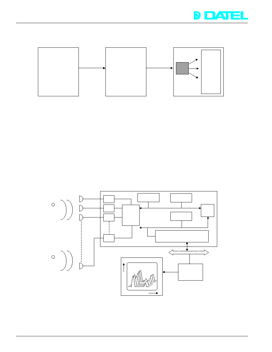
AFB Source Text
Command Script
(written by user)
AFB Binary
Token File
AFB
Token
File
Image
Resident
DSP
Library*
"Parser"
(host side)
Download
to DSP
PCI-431 Memory
*The DSP library was previously downloaded or resident in NVRAM.
Procedure
Calls
Figure 6. AFB Command Script Processing
Source 2
Source 1
A/D
A/D
A/D
A/D
FIFO
Memory
Timebase
Memory
Memory
DSP
PCI Bus Interface
Be
ar
i
n
g
Frequency
Host
Computer
PCI Bus
Sensor
Array
Coherent
Source Fields
Figure 7. Phased Array Sampling
54

PCI-431
Æ
Æ
DATEL, Inc., Mansfield, MA 02048 (USA)
∑
Tel: (508)339-3000, (800)233-2765 Fax: (508)339-6356
∑
Email: sales@datel.com
∑
Internet: www.datel.com
SIGNAL FLOW ARCHITECTURE
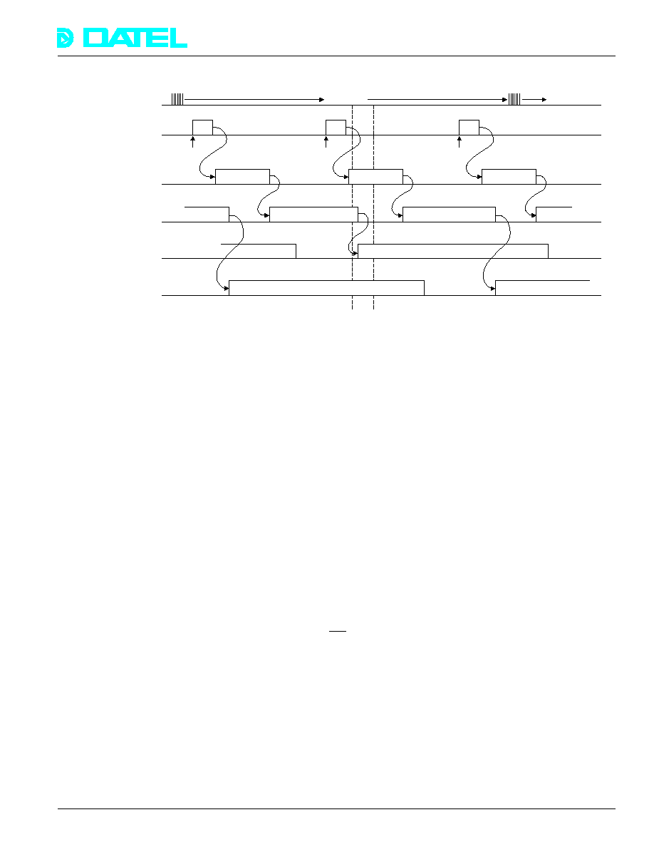
Figure 9. Timing Diagram - Four Simultaneous Processes
This timing diagram shows the PCI-431 as the central controller of a high performance disk storage system. The timing is not to
scale. First, we will assume that all program loading, all memory allocations, and all setup operations before A/D sampling were
previously done and are not shown here. To be complete, we'd also need necessary handshake flags to guard against buffer
overflow or incorrect buffer switching. The arrows connecting from one process to another indicate
causality and connectivity.
That is, the end of one process starts another and is dependent on previous data being ready on time.
A/D data is collected in the usual way to the on-board A/D FIFO memory, triggered by the FIFO half full ("HF") signal. This FIFO
data is periodically moved into DSP memory where the data is immediately processed through a Discrete Cosine Transform
(DCT). The DCT is a standard library function in DATEL's AFB system and on Hyperception RIDE. The DCT compresses the data
into a smaller output array.
Note that the original input data is now discarded. (It will be recovered later after disk playback using
an inverse DCT).
After DCT, the compressed data transfers through the BiFIFO out to host system PCI memory. The PCI-431 acts as a PCI DMA
bus master to make this transfer. A concurrent host program running simultaneously steers these output arrays alternately into
two upper and lower buffers A and B by repeatedly reloading the DMA controller with two swapped addresses. The data then
writes to two separate hard disk drives. Notice that either drive by itself would take too long to collect all the data, therefore two
drives are needed. Also in this example, if the data were not compressed by the DCT, it would be too big to write to the disks in
the time required. This concept is variously called double buffering or swapped buffers and may be extended to several disk
drives in a "round robin" system. This is especially important with small disk systems because disks are much slower than most
A/D boards.
An interesting feature of modern small computer disk systems is that the disk controller will continue to attempt to write data onto
the disk surface
after the Operating System has filled the on-board memory buffer and the BIOS call has returned. Thus the OS
is free to go on to other tasks. We take advantage of this feature by overlapping both the disk writes. In fact, time T1 shows an
extraordinary amount of concurrency and automation with fully four processes running in parallel. The A/D continues sampling
"forever", the DCT is processing, the PCI controller
automatically DMA-transfers out to host memory while buffer A is written to
disk. At time T2, the A/D, DCT and
both disk drives are running simultaneously.
Conclusion
DATEL makes the entire architecture of the PCI-431 open so you can have the highest level of control and performance. The
PCI-431's flexibility is limited only by your imagination. With many years serving a large variety of A/D-DSP applications, DATEL
would like to discuss your ideas.
A/D
clock
A/D FIFO to DSP
memory block transfer
DCT compression
via DSP
DSP upload to host via
PCI DMA from BiFIFO
Write
drive
Write
drive
F:
G:
2K
DCT
Buffer B
Buf A to F:
DMA to Buffer B
Buffer A to Drive F:
Buffer B to Drive G:
DMA to Buffer A
Buffer A
Buf B to G:
"Forever"
HF
2K
HF
2K
HF
T1
T2
Drawing is not to scale
DCT
DCT
55

PCI-431
Æ
Æ
DATEL, Inc., Mansfield, MA 02048 (USA)
∑
Tel: (508)339-3000, (800)233-2765 Fax: (508)339-6356
∑
Email: sales@datel.com
∑
Internet: www.datel.com
ORDERING INFORMATION
Analog Module [1]
A/D Polarity [2]
Global Memory [3]
A = 4 channels, 12 bits
D = 16 chans., 14 bits
1 = bipolar or standard
A = 256k x 32
B = 2 channels, 12 bits
E = 4 chans., 16 bits
2 = unipolar
B = 512k x 32
C = 4 channels, 14 bits
F = 4 chans., 14 bits
C = 1M x 32
L = 16 chans., 12 bits
D = 2M x 32
Example:
PCI-431A1A, 4 A/D channels, 12 bit A/D's, bipolar inputs, 256K x 32 global memory.
UM-PCI-431
Spare user manual. One is included with board.
UM-PCI-431WIN
Spare user manual. One is included with purchase of PCI-431WIN(S) software.
Software [4]:
PCI-431RIDE or PCI-431RIDEL
Hyperception advanced graphical programming library and comprehensive DSP library for
Windows 95 or Windows NT. (PCI-431RIDE provides an extended library of several
hundred functions.) System requirements: Windows 95 or NT, CD-ROM, and 25Mb
spare hard disk space. 16Mb memory or more and Pentium CPU is recommended.
Includes a parallel port security key. DATEL and Hyperception support mutual customers.
PCI-431WIN, PCI-431WINS
Windows 95/98/NT command system. Model PCI-431WIN (executables only) is included
free with the board. The system performs data acquisition, screen FFT's, disk data saves,
PCI bus transfers, and verification of on-board hardware. Full "C" commented source code
is included on PC diskettes as model PCI-431WINS.
PCI-431LV, PCI-431LVS
Model PCI-431LV is DATEL's AFB system fully integrated with LabVIEW 5.1. Includes
bridge driver library of Virtual Instrument incons. LabVIEW must be purchased separately
from National Instruments. Model PCI-431LVS is the source code for the VI bridge
modules only. Purchase model PCI-431WINS for the full AFB source code.
Notes
1. Please refer to the specifications for full information on each analog module type.
2. Some models may have the input polarity selectable by the user. These are designated "standard" (polarity type 1)
even
though the polarity may be either unipolar or bipolar. Please study the specifications.
3. The standard board flash memory is 128k x 16 and the standard local memory is 128k x 32.
4. The AFB executable software is included with the board. Please add other software as needed to your order. Full
application support is available only with board purchase.
Each board is power-cycle burned in, tested and calibrated. The warranty is one year from shipment. All models include a
comprehensive User's Manual.
In accordance with DATEL's policy of product improvement, prices and specifications are subject to change without notice.
Pentium is an Intel trademark
Windows and MS-DOS are Microsoft trademarks
Hypersignal is a Hyperception trademark
LabVIEW is a National Instruments trademark
PCI-431
Hardware:
56
rev. B 1/00
