 | –≠–ª–µ–∫—Ç—Ä–æ–Ω–Ω—ã–π –∫–æ–º–ø–æ–Ω–µ–Ω—Ç: PCI-462 | –°–∫–∞—á–∞—Ç—å:  PDF PDF  ZIP ZIP |

PCI-462
Precision Isolated
Power Supply Board
FEATURES
∑ 4 independently programmable, precision voltage/
current outputs
∑ Remote sensing for all supplies
∑ All channels fully isolated from PCI bus
∑ Output current limits
∑ Real time voltage and current monitoring
∑ 4 general purpose analog inputs
∑ 2 isolated digital inputs
∑ 2 isolated relay driver outputs - MOSFET switches
∑ Comprehensive software with optional source
The PCI-462 is an isolated A/D-D/A board for the desktop PCI bus
featuring four higher current D/A outputs plus A/D current and voltage
monitoring and four general purpose auxiliary A/D inputs. The design
is a PCI bus version of DATEL's PC-462 ISA board retaining identical
performance specifications. Designed for low-cost, medium power
source applications, the PCI-462 is a high-precision, programmable
power supply and sensing board for desktop personal computers.
Four output channels are individually programmable for ranges of 0 to
+6.1425V and 0 to ≠6.1425V at 1A, as well as 0 to +20.475V and 0 to
≠20.475V at 250 milliamps. It is ideal for applications where highly
accurate, very stable DC voltage and current sources are required,
with low ripple and low noise characteristics. All input and output
channels provide 250Vrms isolation from the PCI bus. Combined with
comprehensive, graphic-intensive control software, this quad output
supply card is easily integrated into most automated test and
benchtop power supply applications.
INNOVATION and EX C ELL E N C E
Æ
Æ
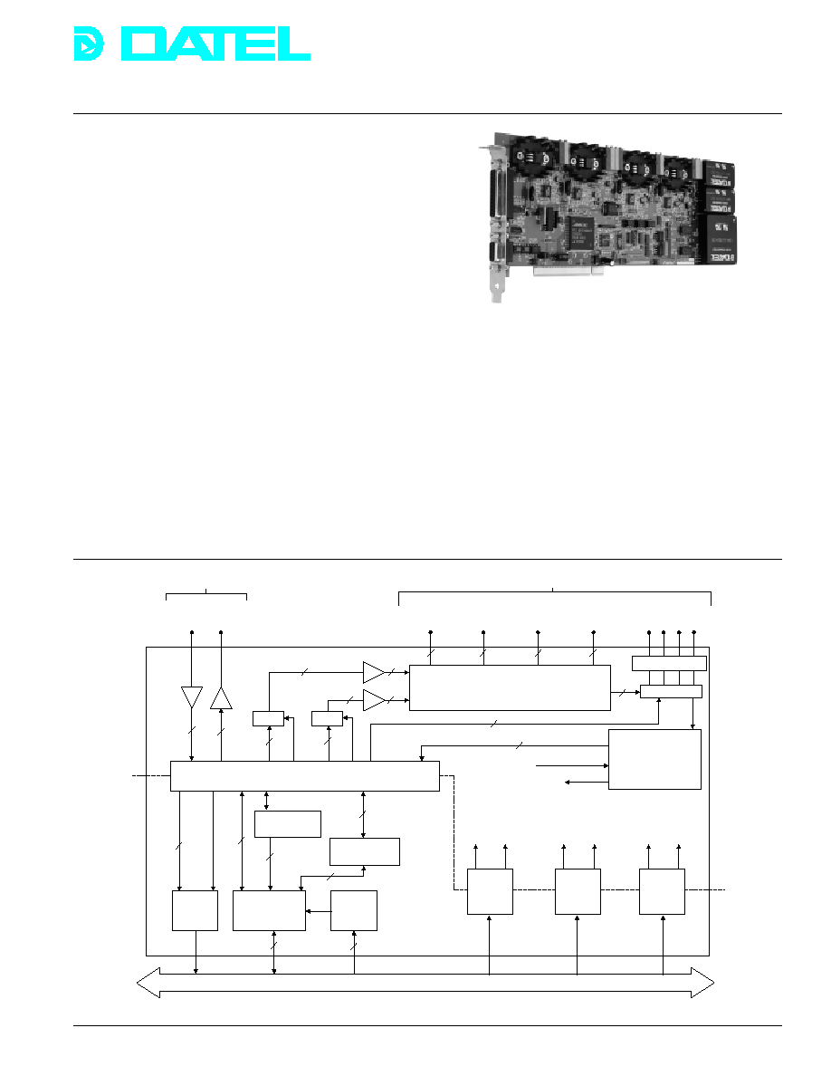
Figure 1. Simplified Block Diagram
DATEL, Inc., Mansfield, MA 02048 (USA)
∑ Tel: (508)339-3000, (800)233-2765 Fax: (508)339-6356 ∑ Email: sales@datel.com ∑ Internet: www.datel.com
1
For dynamic test sequences, the host PC can update all four output
channels in real time. Voltage and current output levels are
continuously monitored by an on-board, 12-bit A/D converter. A rear
panel connector provides an additional 4 auxiliary input channels for
general purpose use. The input range is ±5.12V but component pads
on all of the channels allow for user-selectable ranges as well as
current loop inputs and signal filtering. These channels are fully
isolated from the PCI bus and are ideal for monitoring external
voltage/current conditions in adaptive test applications.
Outputs are protected against overload and short circuit damage by
fixed current limiting circuits. For any overload condition, the
+6.1425V and ≠6.1425V supplies are limited to 1.2A, while the
+20.475V and ≠20.475V supplies are limited to 300 milliamps.
Another protective and very necessary feature is that at power up all
output channels reset to 0V. Remote voltage sensing permits
regulation with respect to the load eliminating problems associated
with lead voltage drops.
2
2
D / A
C o n v e r t e r s
1 2
1 2
C u r r e n t S e n s e
A m p l i f i c a t i o n
M U X
T r a c k i n g
A / D
C o n v e r t e r
2
2
I n t e r r u p t
R e q u e s t
C o n t r o l a n d
S t a t u s R e g i s t e r s
I / O B u s
I n t e r f a c e
B a s e
A d d r e s s
S e l e c t
D i g i t a l
I n 0 , 1
+ 9 V
9 V
+ 2 4 V
+ 1 2 V
2 4 V
1 2 V
+ 5 V
+ 1 2 V
+ 1 2 V
P C I B u s
P 3 C o n n e c t o r
2 M O S . E T O u t p u t s
2 D i g i t a l I n p u t s / E x t . T r i g g e r I n
P 4 C o n n e c t o r
+ 6 . 1 4 4 V
a n d S e n s e
6 . 1 4 4 V
a n d S e n s e
+ 2 0 . 4 8 V
a n d S e n s e
2 0 . 4 8 V
a n d S e n s e
V / I
( G e n e r a l P u r p o s e )
2
2
2
2
C h a n n e l A d d r e s s
4
E O C
A / D D a t a
S T C O N V
P a r a l l e l t o S e r i a l
S e r i a l t o P a r a l l e l
2
E O C
A n a l o g O u t p u t s
I s o l a t i o n
B a r r i e r
H i g h V o l t a g e
O p t o - I s o l a t o r s
D C / D C
P o w e r
C o n v e r t e r
( I s o l a t e d )
D C / D C
P o w e r
C o n v e r t e r
( I s o l a t e d )
D C / D C
P o w e r
C o n v e r t e r
( I s o l a t e d )
D i g i t a l I / O
A n a l o g I n p u t s
S i g n a l C o n d i t i o n i n g
1 2

INNOVATION and EX C ELL E N C E
Æ
Æ
PCI-462
DATEL, Inc., Mansfield, MA 02048 (USA)
∑ Tel: (508)339-3000, (800)233-2765 Fax: (508)339-6356 ∑ Email: sales@datel.com ∑ Internet: www.datel.com
SPECIFICATIONS
(Typical at +25∞C, dynamic conditions, unless noted)
ANALOG OUTPUTS
Number of Channels
Four
Output Configuration
Single-ended with common
isolated analog ground
Full Scale Output Ranges
OUT 1 0 to +6.1425V @ 1A
Max. (See Notes 1 & 4)
OUT 2 0 to -6.1425V @ 1A
OUT 3 0 to +20.475V @250 mA
OUT 4 0 to -20.475V @ 250 mA
Isolation to PCI bus
250 Vrms continuous. See
notes 1 and 2
Isolation Resistance
10 Megohms
Isolation Capacitive
Coupling
850 pF
D/A Output Resolution
12 bits
Input Data Coding
Straight binary, right justified
within 32-bit longword
Channel Addressing Mode
Random channel access via
host software
Output Voltage Accuracy
OUT 1&2: ±0.05% of full scale
Adjustable to Zero
OUT 3 &4: ±0.025% of full scale
Output Settling Time
OUT 1&2: 400 µs max.
to Rated Accuracy
OUT 3&4: 600 µs max.
Output Voltage Slew Rate
1V per µs into 1 µF load
Output Noise,
OUT 1&2: 5 mV max (full load)
dc to 10 kHz
OUT 3&4: 2 mV max (full load)
Output Current Limit
OUT 1&2: 1.2 Amps max.
OUT 3&4: 300mA max.
Output Stability
Unconditionally stable to any
non-active load
Temp. Coefficient
±20 ppm of FSR per
degree Celsius
OUTPUT PERFORMANCE
2
Four isolated digital I/O lines are available to monitor and
control external devices. The two input lines may be
configured to generate interrupt requests to the host computer
possibly indicating an external error condition or failure and
requesting immediate system attention. One of these lines is
software selectable as an A/D digital trigger input. The two
MOSFET output lines can switch up to 300V at 100 milliamps
for an indefinite period of time. These outputs are ideal for
switching heavy external loads such as relays, triacs, etc.
The PCI-462 is configured on a full size PCI card and it is
completely contained within the host computer. The direct bus
interface increases the output slew rates and decreases the
host response time to read back voltage/current data. All
isolated input and output channels are available on two D-type
connectors on the rear panel. The board is compatible with
most popular programming languages and all data is right
justified to facilitate integer data typing with high level
languages. A comprehensive User's Manual details full
installation, programming, and application information.
ANALOG INPUTS
Number of Channels
16 (4 general purpose auxiliary
external user inputs, 12 for internal
monitoring)
Internal Monitor Inputs
OUT 1-4 voltage out, OUT 1-4
current out, +5.12V ref., ≠5.12V ref.,
ground reference
External User Analog
Inputs
4 channels, ±5.12V input range
External Inputs
Configuration
Single-ended with common
isolated analog ground (single A/D
converter plus analog multiplexer)
Isolation to PCI bus
250 Vrms continuous, see notes 1
and 2
External Inputs
DC Accuracy
±0.025% of full scale range ±1 LSB
External Inputs
Impedance
10 megohms minimum
External Inputs
Bias Current
±500 nanoamps
External Inputs
Capacitance
1000 pF in series with 2 kilohms
External Inputs
Overvoltage
±6V sustained max., no damage
see note 7
Channel Addressing
Modes
Random channel access via host
software
Resolution
12 bits
A/D Conversion Time
50 microseconds
A/D Output Coding
Two's comp. bipolar (1 sign bit, 11
data) right justified within 32-bit
longword (no sign extension)
A/D Sample Clock
Selectable from user's external
logic input or by program register
write
External A/D Clock
20 µs min. width, starts on falling
Input
edge, TTL levels, non-isolated
Number of Channels
2 bits, isolated non latched
Isolation from PCI bus
250 Vrms continuous, note 2
Input Current
0 mA for logic ZERO, 10 mA for
logic ONE, TTL levels
Input Delay Time
20 µs
DIGITAL INPUTS
A/D CONVERTER

INNOVATION and EX C ELL E N C E
Æ
Æ
PCI-462
DATEL, Inc., Mansfield, MA 02048 (USA)
∑ Tel: (508)339-3000, (800)233-2765 Fax: (508)339-6356 ∑ Email: sales@datel.com ∑ Internet: www.datel.com
DIGITAL OUTPUTS
Number of Channels
Two channels
Output Type
MOSFET power switches, passive.
External excitation required.
Output Rating
300V, 100 mA continuous.
Minimum Excitation
Voltage
3V
Isolation to PCI bus
250 Vrms see note 2
FET Switch ON
Resistance
25 Ohms
Switch Time
1 millisecond
PCI bus Controller
Type
AMCC 5920
Data Path
32 bits (the upper 16 bits are not
used)
PCI bus Interrupts
Selectable as INTA (default), INTB,
INTC, or INTD
Interrupt Source
Selectable from:
1 - A/D End of Conversion
2 - Digital input channel 0 LOW
3 - Digital input channel 1 LOW
Analog Connector
Rear panel DB-25 female 25-pin,
same as PC-462
Digital Input/Output
Rear panel DB-9 female 9-pin,
same as PC-462
Power Required
+5Vdc at 4 Amps max. and +12V
at 1.5 Amps max. from PCI bus,
note 4
Operating Temp. Range
0 to 50∞C forced cooling is required
Storage Temp. Range
-25 to +85∞C
Relative Humidity
10% to 90%, non-condensing
Altitude
0 to 10,000 ft
Outline Dimensions
4.5" (bottom of edgeboard fingers
to top of PC board) x 12.313" (total
PC board length, not including
connectors) x 0.5"
Fabrication
Multilayer printed circuit board with
surface mount components.
Caution: Do not flex board or
apply mechanical stress
Manufacturing
Environment
ISO 9001 certified facility and
procedures
3
PCI BUS INTERFACE
CONNECTORS
MISCELLANEOUS
TECHNICAL NOTES
1.
To sensitive outside circuits, the analog isolation grounds
may exhibit low levels of computer bus clock signals and
very low level DC/DC power converter switching spikes.
From outside circuits, do not drive the isolation barrier with
AC voltages beyond 250Vrms and 60 Hz (lower AC drive
results in better data quailty). Do not induce
any spike
or hash noise which can capacitively couple across the
isolation barrier. Failure to observe this lImit may induce
data and control errors. The board may be jumpered as
non-isolated to eliminate ground noise.
2. The A/D and D/A sections share a common isolated
return. This same isolated return is ohmically connected
to the isolated digital I/O ground. Observe proper current
return and sense wiring.
3. The digital outputs require external excitation for operation.
4. Provide adequate PCI bus power and position the board
nearest the power supply. At high D/A currents, insufficient
PCI power could induce data errors. The PCI-462 makes
no connection to +3.3V PCI bus power.
5. Recalibration is recommended at 90 day intervals,
depending on operating conditions.
6. Adjustments: A/D offset and gain, D/A gain and offset.
7. Caution: Do not allow spike inputs to the A/D auxiliary
inputs. Install external voltage clamping if necessary.

INNOVATION and EX C ELL E N C E
Æ
Æ
PCI-462
DATEL, Inc., Mansfield, MA 02048 (USA)
∑ Tel: (508)339-3000, (800)233-2765 Fax: (508)339-6356 ∑ Email: sales@datel.com ∑ Internet: www.datel.com
A/D Data Format:
Bits 31 to 12
Bit 11 (MSB*)
Bits 10 to 0 (LSB)
Not used
2's complement polarity
11 A/D data bits
REGISTER INTERFACE
The PCI-462 uses the same basic registers as its PC-462 ISA
bus predecessor but uses an Applied Micro Circuits Corp.
(AMCC - San Diego, CA 800-755-2622, www.amcc.com)
S5920 PCI controller to connect internal PCI-462 registers to
the PCI bus. These internal registers are mapped to
PassThru
(PT) Regions in accordance with the PCI bus specification.
These PT Regions are pointed to by the contents of the Base
Address Registers (BADRx) in the S5920. Consult the AMCC
S5920 Controller Manual (www.amcc.com/Products/PCI/
S5920/.htm) for full information on the S5920. The PCI-462
uses BADR1 and above. BADR0 is reserved for S5920
internal operations.
The absolute I/O addresses of these PT regions are estab-
lished by the PCI BIOS at the time of initialization and placed
in the BADR's.
Access Speed: The PCI-462 interface logic is set up so that
different access delays are available depending on which PT
region is addressed. This is done to accommodate some
slower logic on the board requiring longer setup time and
propagation delays for reliable operation. This is
not done to
provide delays for the opto isolators. The access delays are
on the order of a few PCI 33 MHz clocks.
The selectable delay feature means that any one register will
be mapped in multiple PT areas, each with a different access
speed. Note particularly that the access delay is selected
solely by using the correct (BADRx) I/O address mapped for
that PT region.
Architecture: The PCI-462 is intended for medium speed non-
streaming applications and does not use any on-board data
memory or FIFO's as with other DATEL boards. Essentially, if
you write to a D/A register, analog signals appear a short time
later (the settling delay plus opto isolator delays). And for the
A/D section, if you need current data, you must keep reading
the data register using the EOC protocol specified below.
There is no on-board data storage. Because of the high speed
of the PCI bus, it is possible to overrun the isolated register
interface of the PCI-462 if you make access too fast. You may
need software delays. Use the published conversion and
settling rates as an initial guide.
Also note that several registers are co-located at the same
address. However, these are physically different read and
write registers. With some exceptions, you cannot read back
the write-only registers. You must maintain a
shadow register
in your program to remember what you wrote. If you read
back write-only registers, you will get meaningless data or
undefined operation.
4
All registers require 32-bit DWORD access even though less
than 32 bits are used. These bits are right justified starting
from bit 0.
Listed below is a summary of the PCI-462 Registers.
Register Name
PCI Address
Access
Command Register
PT Region X+0
Write only
Status Register
PT Region X+0
Read only
Channel Address Register
PT Region X+4
Write only
DAC Data Register
PT Region X+8
Write only
Start A/D Convert Register
PT Region X+12
Write only
A/D Data Register
PT Region X+12
Read only
COMMAND REGISTER
31 - 5
4 3
2
1
0
Not
Interrupt
A/D Clock
Digital
Digital
Used
Source
Select
Out 1
Out 0
Note that the interrupt source is not the same as the PCI bus
interrupt request line selected by P6.
STATUS REGISTER
31 - 5
4 3
2
1
0
Not
Interrupt
A/D EOC
Digital
Digital
Used
Source
Status
In 1
In 0
Interrupt Source The Interrupt Source status bits 4 and 3
(Bits 4,3)
echo the selection made in Command bits
4 and 3. This may be used to verify the bus
interface by masking off all other bits before
other functions are tested.
A/D EOC Status 0 = A/D is busy converting. Data is not valid.
(Bit 2)
1 = A/D has not started converting yet or
conversion is done and data is valid.
The A/D End of conversion (EOC) status bit 2 takes a small
delay after start of conversion to transition from ONE to ZERO
(busy converting). It returns to ONE (conversion done, data is
ready) when conversion is complete. It may briefly indicate
ONE before the start of conversion, thereby falsely implying
that data is ready if you read it too quickly after starting
conversion.
CHANNEL ADDRESS REGISTER
31 - 5
7 - 4
3 2
1 0
Not
A/D Channel
Not
D/A Channel
Used
Select
Used
Select
D/A DATA REGISTER
31 - 12
11
10 - 1
0
Not
D/A Bit 1
D/A Bits
D/A Bit 12
Used
(MSB)
2-11
(LSB)

INNOVATION and EX C ELL E N C E
Æ
Æ
PCI-462
DATEL, Inc., Mansfield, MA 02048 (USA)
∑ Tel: (508)339-3000, (800)233-2765 Fax: (508)339-6356 ∑ Email: sales@datel.com ∑ Internet: www.datel.com
5
START A/D CONVERT REGISTER
31 - 0
Data is
"don't care"
Write any data to this register to start an A/D conversion
if
Command Bit 2 = 0 (internal A/D start). All previous A/D data
will be lost if it is not read before the next start.
A/D DATA REGISTER
31 - 12
11
10 - 1
0
Not
A/D Bit 1
A/D Bits
A/D Bit 12
Used
(MSB)
2-11
(LSB)
JUMPERS, BOARD FEATURES, AND ADJUSTMENTS
PCI bus Interrupt Selection - P6
Interrupt
Close Jumper
INTA (standard default)
7 to 8
INTB
5 to 6
INTC
3 to 4
INTD
1 to 2
Leave all other interrupt jumpers open.
ISP Programming Port - P2
Make no connection.
Isolated Ground Connection - Jumpers JP2 to JP7
Normally these jumpers are open to retain isolation between
the two ground systems. If isolation is not desired, insert
jumpers at pins 1 and 2 for all of JP2 to JP7. All jumpers are in
parallel however for lowest noise, install
all jumpers.
Analog Input Dividers
Each of the auxiliary analog inputs, AUXIN1 through AUXIN4
offer an on-board voltage divider to accommodate either
current shunts or limited scaling to higher input voltage ranges.
The circuits consist of a 2000 ohm series SMT resistor (always
installed) from the external inputs with a second shunt resistor
from the acutal multiplexer input to ground as the bottom leg
(the shunt) of the voltage divider. The shunt resistors are not
installed on standard units and must be surface mount. Note
that standard surface mount rsistors are normally not precision
types. The 2Kohm series resistors offers limited protection
against overvoltages. DATEL will change either value for
custom quantity orders.
Analog Channel
Series Resistor
Shunt Resistor
(normally 2Kohms)
AUXIN1
R42
R24
AUXIN2
R41
R25
AUXIN3
R40
R37
AUXIN4
R39
R38
D/A Adjustments
Channel
Offset Adjust
Full Scale Adjust
+6V
R52
R55
≠6V
R53
R54
+20V
R92
R95
≠20V
R93
R94
R5 is a trim for the +5.12Vdc reference which appears at U2-6.
The ≠5.12V reference appears at U14-6. Normally this
adjustment should not be changed.
A/D Adjustments
R21: Offset adjust
R20: Full scale adjust
REAR PANEL INPUT/OUTPUT CONNECTIONS
All input and output connections are made using two female
connectors on the rear mounting panel. P1 is a 25-pin, DB-
25S connector for all load conections to the PCI-462 output
channels. P1 also includes the four auxilliary, general purpose
analog input connections.
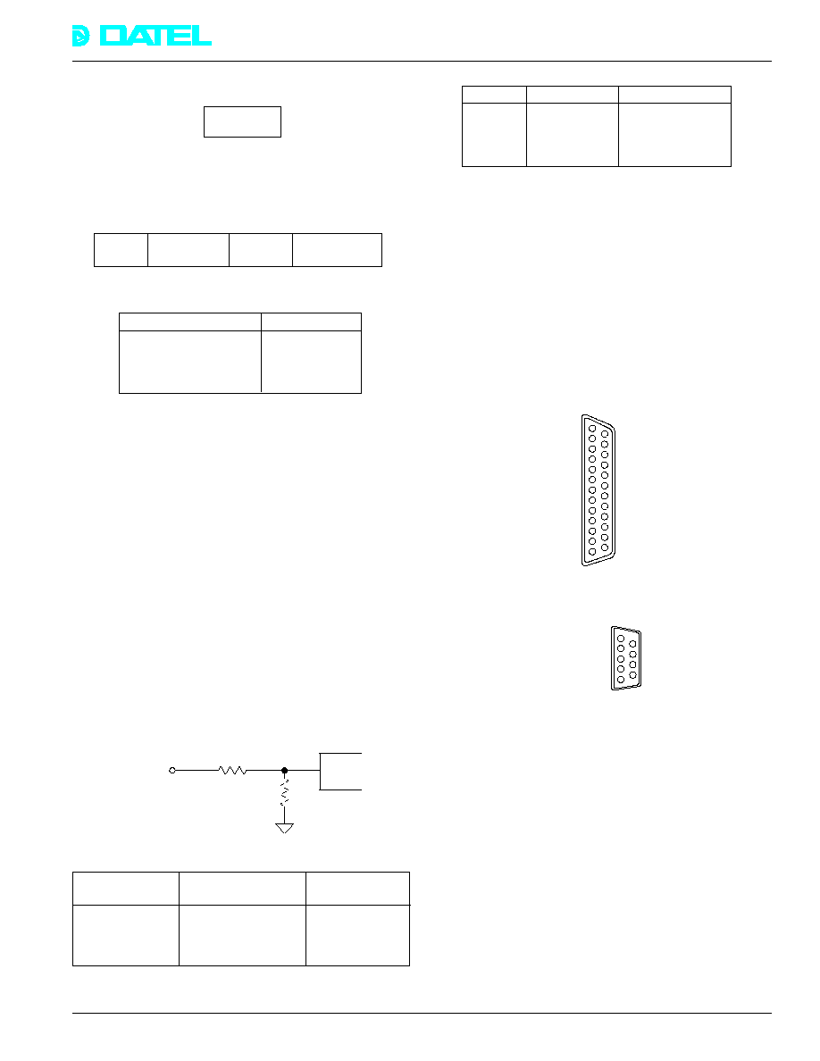
Figure 2. Voltage/Current Outputs, Analog Inputs - P4
Figure 3. Isolated Digital Port - P3
Isolated Digital Port Connector - P3
This is a rear panel 9 pin DB9S connector (socket, female).
Viewed from the rear panel, pin 1 is to the lower right.
6: Relay Out 1B 7: Relay Out 2B 8: Digital In 1 LO 9: +5Vdc
out, 1A
1: Relay Out 1A 2: Relay Out 2A 3: Digital In HI 4:Extrn
Trig/Dig. In 0 LO 5: Digital Ground
1
2
3
4
5
6
7
8
9
1 0
1 1
1 2
1 3
+ 6 . 1 4 2 5 V O U T
+ 6 . 1 4 2 5 V O U T
+ 6 . 1 4 2 5 V S E N S E I N
6 . 1 4 2 5 V O U T
6 . 1 4 2 5 V O U T
– 6 . 1 4 2 5 V S E N S E I N
+ 2 0 . 4 7 5 V O U T
+ 2 0 . 4 7 5 V S E N S E I N
2 0 . 4 7 5 V O U T
2 0 . 4 7 5 V S E N S E I N
A N A L O G I N P U T C H A N N E L 1
A N A L O G I N P U T C H A N N E L 3
A N A L O G R E T U R N
1 4
1 5
1 6
1 7
1 8
1 9
2 0
2 1
2 2
2 3
2 4
2 5
+ 6 . 1 4 2 5 V R E T U R N
+ 6 . 1 4 2 5 V R E T U R N
+ 6 . 1 4 2 5 V R E T U R N S E N S E
6 . 1 4 2 5 V R E T U R N
6 . 1 4 2 5 V R E T U R N
6 . 1 4 2 5 V R E T U R N S E N S E
+ 2 0 . 4 7 5 V R E T U R N
+ 2 0 . 4 7 5 V R E T U R N S E N S E
2 0 . 4 7 5 V R E T U R N
2 0 . 4 7 5 V R E T U R N S E N S E
A N A L O G I N P U T C H A N N E L 2
A N A L O G I N P U T C H A N N E L 4
R E L A Y O U T 1 A
R E L A Y O U T 2 A
D I G I T A L H I G H I N
E X T . T R I G G E R / D I G I T A L I N 0 L O
D I G I T A L G R O U N D
1
2
3
4
5
6
7
8
9
R E L A Y O U T 1 B
R E L A Y O U T 2 B
D I G I T A L I N 1
+ 5 V @ 1 A m p m a x .
2 k
External
Analog
Input
Analog
MUX

INNOVATION and EX C ELL E N C E
Æ
Æ
PCI-462
DATEL, Inc., Mansfield, MA 02048 (USA)
∑ Tel: (508)339-3000, (800)233-2765 Fax: (508)339-6356 ∑ Email: sales@datel.com ∑ Internet: www.datel.com
LOAD CONNECTIONS
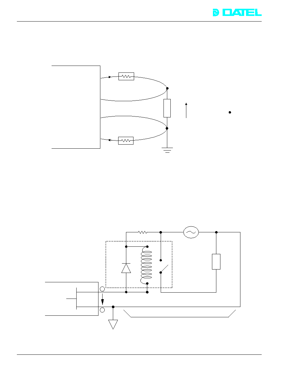
Figure 2 illustrates a typical load connection to one of the output channels. Make sure that the SENSE OUT and SENSE
RETURN connections are completed so that the voltage across the load is exactly the required value. This remote voltage/current
sensing facility eliminates attenuation errors due to lead resistance voltage drops. The feedback loop adapts the PCI-462 output
level so that the load voltage is regulated to the desired value, i.e. lead attenuation is cancelled. Note that there are no voltage
drops on the SENSE IN or the V
RET
lines since no current flows through them.
Note: The voltage across the load is the true value. The voltage at the P4 connector (V
OUT
) will be somewhat higher (±1V max.)
to compensate for lead attenuation
Figure 4. Typical Load Connections
MOSFET OUTPUT CONNECTIONS
The two isolated MOSFET output lines may be used to switch heavy loads or drive standard TTL level devices. Figure 5a illustrates a
typical connection to a solid state relay. The relay in turn may switch higher rated loads - in excess of 300V, 100 milliamps.
Figure 5a. Typical MOSFET Output Switching a Relay
V
O U T
S E N S E
I N
V
R E T U R N
S E N S E
R E T U R N
R
L E A D
R
L E A D
I
R E T
I
O U T
R
L O A D
V
L O A D
= V
O U T
I
O U T
R
L E A D
P C I - 4 6 2
P 4
C o n n e c t o r
I m p o r t a n t : C o n n e c t t h e s e n s e o u t p u t s a t t h e l o a d .
A
B
1 2 0 m A m a x .
C u r r e n t
L i m i t i n g
R e s i s t o r
H e a v y
L o a d
C l a m p
D i o d e
P o w e r
S o u r c e
M O S . E T
S w i t c h
R e l a y
P 3 C o n n e c t o r
o n P C I - 4 6 2
3 5 0 V
m a x .
+
U s e r ' s e x t e r n a l c i r c u i t ( t y p i c a l )
6

INNOVATION and EX C ELL E N C E
Æ
Æ
PCI-462
DATEL, Inc., Mansfield, MA 02048 (USA)
∑ Tel: (508)339-3000, (800)233-2765 Fax: (508)339-6356 ∑ Email: sales@datel.com ∑ Internet: www.datel.com
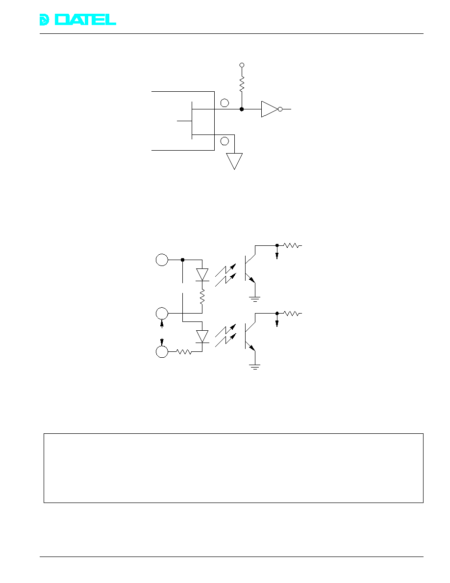
Standard TTL gates and logic devices may be driven by pulling up the digital output lines to the +5 rail through a resistor
Figure 5b. MOSFET Output Driving TTL Load
Figure 6. Digital Inputs
ORDERING GUIDE
Model
Description
PCI-462
Programmable power supply board. Includes a comprehensive user's Manual and low level driver
library on PC-CDROM (has all binaries, no sources).
PC-CDROMS
Complete source code to setup/configuration utility on CD-ROM. Runs under all Windows versions.
Includes Plug-n-Play, ActiveX controls, visual BASIC example and LabVIEW.Æ
PC-490A/-490B
Screw termination adapter to facilitate input/output wiring (490A DB-9, 9-pin, 490B DB-25, 25-pin)
A
B
+ 5 V
4.7 K
Pullup
T T L G a t e
M O S . E T
S w i t c h
P 3 C o n n e c t o r
o n P C I - 4 6 2
+
E x t e r n a l c o n n e c t i o n s
I N H I
I N L O 0
I N L O 1
I s o l a t i o n
B a r r i e r
+ 5 V
T o s t a t u s r e g i s t e r
a n d i n t e r r u p t
3
8
4
P 3 C o n n e c t i o n s
330
330
+ 5 V
T o s t a t u s r e g i s t e r
a n d i n t e r r u p t
7
LabVIEW is a National Instruments trademark. Windows and ActiveX are Microsoft Corp. trademarks.
Rev. B 1/02
