PCI-466
96-Line, TTL-Level Digital I/O
Board for Desktop PCI Bus
INNOVATION and EX C ELL E N C E
Æ
Æ
FEATURES
∑∑
∑∑
∑
96 TTL/CMOS compatible digital I/O lines
∑∑
∑∑
∑
Programmable in or out in 8 bit groups
∑∑
∑∑
∑
External PCI bus interrupt
∑∑
∑∑
∑
Direct interface to wide range of accessory products
∑∑
∑∑
∑
Brings out fused ±5V dc power from bus
∑∑
∑∑
∑
Programmable front panel LED lamp
The PCI-466 provides 96 TTL/CMOS compatible digital input/
output lines for a wide variety of digital I/O applications. The
board also includes access to the PCI bus interrupt inputs and
also includes connections to the computer's power supplies
with the addition of a ≠5 VDC supply and field replaceable
fuses.
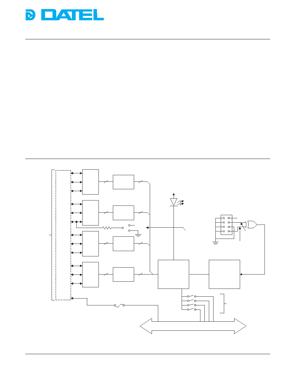
On the PCI-466, four industry standard 82C55 programmable
peripheral interface (PPI) controllers provide 96 digital I/O
lines. The PCI-466 runs the 82C55's in mode 0.
The 96 digital I/O lines of the PCI-466 form twelve separate 8
bit ports. These ports can be set independently under
software control as inputs or outputs. All ports are configured
as inputs on power-up or reset.
Figure 1. Simplified Block Diagram
DATEL, Inc., Mansfield, MA 02048 (USA)
∑
Tel: (508)339-3000, (800)233-2765 Fax: (508)339-6356
∑
Email: sales@datel.com
∑
Internet: www.datel.com
PRELIMINARY PRODUCT DATA
A separate circuit handles PCI bus interrupts and has
programmable polarity. This driver can be connected to any of
the interrupt levels `A' through `D' available on the PCI bus.
The PCI-466 includes a Windows 95/98 and Windows NT
control panel. Also available are sample programs, source
code, and an ActiveX control for all popular programming
languages and packages.
PCI
bus
Controller
Programmable
Logic
Internal
Optional
Activity Indicator
(yellow lamp)
+5 VDC @ 0.25A
82C55
82C55
82C55
82C55
+5V
+5V
10 k
Programmable
Pull up/down
(96 lines)
Interrupt
Polarity
External
Interrupt
Input
Desktop PCI Bus
P5
Header
S1
A
B
C
D
Interrupt
Select
100 pin
Rear Panel
Connector
Parallel
Controllers
Transceive rs
12
Byte-wide
Ports
JP1
2
1
1
4
3
8
7
2
1

PCI-466
DATEL, Inc., Mansfield, MA 02048 (USA)
∑
Tel: (508)339-3000, (800)233-2765 Fax: (508)339-6356
∑
Email: sales@datel.com
∑
Internet: www.datel.com
INNOVATION and EX C ELL E N C E
Æ
Æ
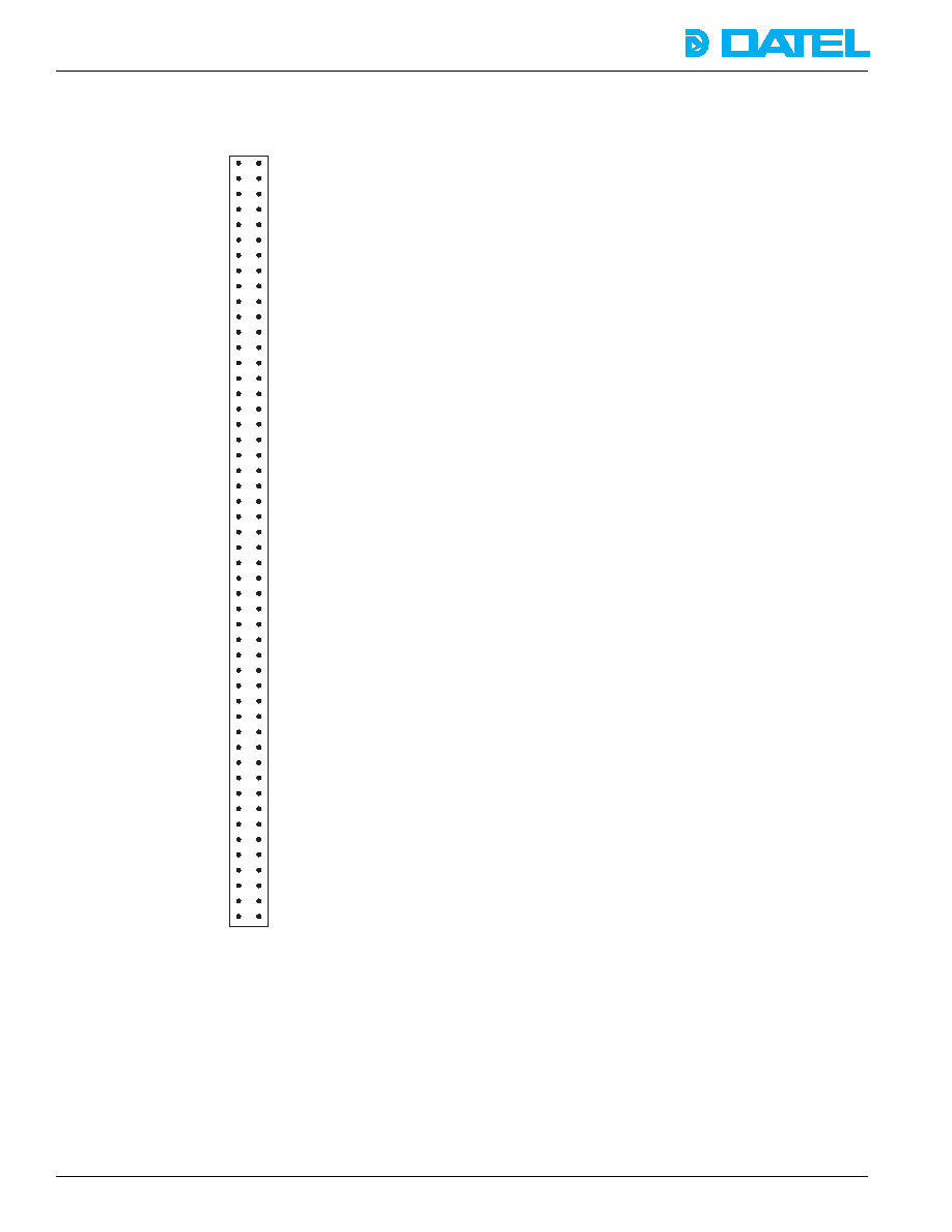
Input Output Connector
The I/O connector for the PCI-466 is a high density 100 pin
type and is accessible at the rear of the PCI chassis.
Figure 2. I/O Connector
Input/Output Connections
The digital data bits are arranged in four ports (0 through 3)
organized around the four 82C55 controllers. Each port
contains 24 non-isolated digital I/O lines from the three bytes
in each controller. The bytes are labelled A, B, and C
corresponding to their designation in the controller registers.
(CAUTION: The grounds are shared with the computer power
supply bus common.)
Assuming that the data direction is previously set, data is valid on
the outputs within 500 nanoseconds after writing from the PCI
bus. Data may be read by the PCI bus within 500 nanoseconds
after data is placed on the lines. No latch or strobe controls are
used. If you need hardware latch controls, refer to DATEL's
PCI-469 parallel I/O board. Or the separate external PCI
interrupt input may be configured as a software input latch.
Unlike the stock 82C55 controller, each data line is rated at 8 mA
for output, considering the worst case where all bits are on or off.
For fewer number of connected bits or not all bits high or low, up
to 24 mA is available per line. Pins 49 and 99 offer fused +5 Vdc
at 250 mA maximum power each for external, user-supplied
functions.
All port bytes default to
inputs on power up. Also, all lines will
accept user-supplied 10 Kilohm pullup resistors in 8 bit
groups to force the inputs to either logical ZERO's or ONE's if
they are not terminated.
Pins 50 and 100 serve as digital grounds for the data pins.
Generally, there is very little current through each bit therefore
these two grounds are sufficient. If you need additional
grounding and are not using the +5V power lines, consider
removing the fuses for pins 49 and 99 then wiring digital
ground to the connector end of these fuses.
Do not reinstall
the fuses!
Programming
The PCI-466 is mapped in I/O space. Because of the slot
addressing feature of the PCI bus, several PCI-466 boards
may be used on the same PCI bus offering hundreds of
programmable I/O bits in one computer. After using the
Configuration Space BIOS functions in the computer, the
contents of the Base Address Registers (BADRx) on the
board may be read. The appropriate BADR contains the base
of the absolute I/O address of the internal registers as "Pass
Through" (PT) regions. The PCI-466 uses BADR1 as primary
I/O line access.
Each data byte occupies the least significant eight bits (7-0) of
a 32-bit longword. The upper bits 31-8 are not used. All
access requires longword addressing. Each byte may be
accessed separately and has its own offset address from the
Base Address. However, all bits within each byte A or B must
be assigned as either read or write. The whole byte may be
programmed on the fly as read or write. Byte C on each
controller may be programmable as split input or output by 4-
bit nybbles according to the 82C55 mode 0 control functions.
Thus it is possible for example to have 12 inputs and 12
outputs on each 82C55.
Since access through the PCI bus requires a finite amount of
time, for highest speed keep a "shadow register" variable in
memory which stores the last value written to each outport.
Or in output mode, you may read the previous byte sent from
the controller. To change the state of one output bit, process
the shadow register first for that bit then write the whole byte
out to the longword address.
You cannot permanently assign base addresses to the
PCI-466 and there are no on-board switches to do this, unlike
older ISA and VME boards. If you add, remove, or reposition
more boards to your computer, these absolute base
addresses may change since they are controlled by the PCI
Plug and Play BIOS function. Therefore
always use the PCI
BIOS access to determine the slot number and base address
of the board
each time you reboot.
Port 2, Bit A7 75
25 Port 0, Bit A7
Port 3, Bit C0 74
24 Port 1, Bit C0
Port 3, Bit C1 73
23 Port 1, Bit C1
Port 3, Bit C2 72
22 Port 1, Bit C2
Port 3, Bit C3 71
21 Port 1, Bit C3
Port 3, Bit C4 70
20 Port 1, Bit C4
Port 3, Bit C5 69
19 Port 1, Bit C5
Port 3, Bit C6 68
18 Port 1, Bit C6
Port 3, Bit C7 67
17 Port 1, Bit C7
Port 3, Bit B0 66
16 Port 1, Bit B0
Port 3, Bit B1 65
15 Port 1, Bit B1
Port 3, Bit B2 64
14 Port 1, Bit B2
Port 3, Bit B3 63
13 Port 1, Bit B3
Port 3, Bit B4 62
12 Port 1, Bit B4
Port 3, Bit B5 61
11 Port 1, Bit B5
Port 3, Bit B6 60
10 Port 1, Bit B6
Port 3, Bit B7 59
9 Port 1, Bit B7
Port 3, Bit A0 58
8 Port 1, Bit A0
Port 3, Bit A1 57
7 Port 1, Bit A1
Port 3, Bit A2 56
6 Port 1, Bit A2
Port 3, Bit A3 55
5 Port 1, Bit A3
Port 3, Bit A4 54
4 Port 1, Bit A4
Port 3, Bit A5 53
3 Port 1, Bit A5
Port 3, Bit A6 52
2 Port 1, Bit A6
Port 3, Bit A7 51
1 Port 1, Bit A7
Digital Ground 100
+5V dc power out, 0.25A max. 99
Port 2, Bit C0 98
Port 2, Bit C1 97
Port 2, Bit C2 96
Port 2, Bit C3 95
Port 2, Bit C4 94
Port 2, Bit C5 93
Port 2, Bit C6 92
Port 2, Bit C7 91
Port 2, Bit B0 90
Port 2, Bit B1 89
Port 2, Bit B2 88
Port 2, Bit B3 87
Port 2, Bit B4 86
Port 2, Bit B5 85
Port 2, Bit B6 84
Port 2, Bit B7 83
Port 2, Bit A0 82
Port 2, Bit A1 81
Port 2, Bit A2 80
Port 2, Bit A3 79
Port 2, Bit A4 78
Port 2, Bit A5 77
Port 2, Bit A6 76
50 Digital Ground
49 +5V dc power out, 0.25A max.
48 Port 0, Bit C0
47 Port 0, Bit C1
46 Port 0, Bit C2
45 Port 0, Bit C3
44 Port 0, Bit C4
43 Port 0, Bit C5
42 Port 0, Bit C6
41 Port 0, Bit C7
40 Port 0, Bit B0
39 Port 0, Bit B1
38 Port 0, Bit B2
37 Port 0, Bit B3
36 Port 0, Bit B4
35 Port 0, Bit B5
34 Port 0, Bit B6
33 Port 0, Bit B7
32 Port 0, Bit A0
31 Port 0, Bit A1
30 Port 0, Bit A2
29 Port 0, Bit A3
28 Port 0, Bit A4
27 Port 0, Bit A5
26 Port 0, Bit A6

PCI-466
DATEL, Inc., Mansfield, MA 02048 (USA)
∑
Tel: (508)339-3000, (800)233-2765 Fax: (508)339-6356
∑
Email: sales@datel.com
∑
Internet: www.datel.com
INNOVATION and EX C ELL E N C E
Æ
Æ
PCI-466WIN Software
Each PCI-466 includes installation software for hardware
detection and initialization under Windows 95/98 and Windows
NT. The control panel provides an easy to use, point and click
graphical user interface (GUI) allowing access to 82C55, port
direction configuration, and reading and writing data.
PCI-466WINS
The PCI-466WINS includes all the features of the PCI-466WIN
software plus the complete source code to the GUI application
(Microsoft Visual Basic) and DLLs (Visual C++), and allows you
to communicate with the PCI-466 from the familiar environment
of your favorite high level language - C/C++, Visual Basic,
LabVIEW
Æ
, etc. Its standard Windows programming hierarchy
facilitates custom software development of the PCI-466 into
other applications. The source code also contains some simple
example programs in Visual Basic, Visual C++, and National
Instruments' LabVIEW.
LabVIEW
Æ
Support
Included with the PCI-466WINS, is information on how to
convert the PCI-466 ActiveX control to a LabView VI (Virtual
Instrument) that allows complete hardware control under
LabVIEW. This software also allows for the control of multiple
PCI-466s in one system and includes complete functional VI
sample programs.
Number of I/O lines
96 programmable input or
output in 8 bit bytes
Controller
Four 82C55 PPI, mode 0 only
Input Logic Low Voltage
≠0.5V min., +0.8V max.
Input Logic High Voltage
2.0V min., 5.0V max.
Input I
load
≠10 µA min., +10 µA max.
Input Low Current,
Interrupt Inputs
≠0.04 mA
Input High Current,
Interrupt Inputs
+20 µA
Output I
sink
(VOL = 0.45V)
8 mA max.
Output I
source
(VOH = 2.4V)
8 mA max.
Settling Time
500 nanoseconds
Compatibility
TTL, LSTTL levels
Internal LED
User-programmable lamp
Front Panel Connector
100 pin high density
PCI Controller
AMCC S5920
Interrupts
An external interrupt input may
generate a PCI bus interrupt.
Interrupt Line
Int A, B, C, or D (user
selectable)
Outline Dimensions
Desktop PCI 7.5" x 3.88"
Operating Temp. Range
0 to +60∞C, non-condensing
Storage Temp. Range
≠25 to +85∞C
Power Supply
+5V dc @ 1A from PCI bus
ORDERING INFORMATION
PCI-466
96 bit digital I/O board for the PCI bus
with user manual and PCI-466WIN
software.
PCI-466WIN
Windows 95/98/NT software application
for the PCI-466. Includes a Windows
device driver and DLLs. (Included with
PCI-466.)
PCI-466WINS
Source code for PCI-466WIN. Includes
the source code to the GUI application
(Microsoft Visual Basic) and DLL sources
(Visual C++), plus sample programs in
C/C++, Visual Basic, and National
Instruments' LabVIEW and access to
ActiveX control.
PC-100CBL
Mating cable, 1M, 100-pin to two 50-pin
flat cable sockets.
FUNCTIONAL SPECIFICATIONS
(typical at +25∞C unless noted)
LabVIEW is a National Instruments trademark
Windows is a Microsoft Corporation trademark
Rev. A 6/01
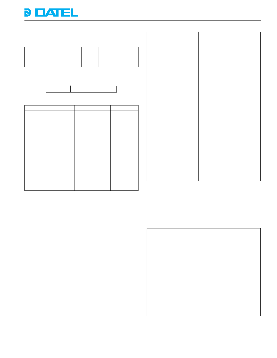
Control Register
The Control Register for each 82C55 sets the direction in or out
for each byte. Bit 7 must always be ONE. Allowable codes are:
Bits 7-5
Bit 4
Bit 3
Bit 2
Bit 1
Bit 0
1-0-0
Byte A:
Byte C
0
Byte B:
Byte C
1=in
bits 7-4:
1=in
bits 3-0:
0=out
1=in
0=out
1=in
0=out
0=out
Register Format
Bits 31-8
Bits 7-0
Not used
Data or Control Byte
Register Mapping
Register Name
PCI Address
Access
Port 0, Byte A
PT Base + 0
Read/Write
Port 0, Byte B
PT Base + 4
Read/Write
Port 0, Byte C
PT Base + 8
Read/Write
Port 0, Control Register
PT Base + 0Ch
Read/Write
Port 1, Byte A
PT Base + 10h
Read/Write
Port 1, Byte B
PT Base + 14h
Read/Write
Port 1, Byte C
PT Base + 18h
Read/Write
Port 1, Control Register
PT Base + 1Ch
Read/Write
Port 2, Byte A
PT Base + 20h
Read/Write
Port 2, Byte B
PT Base + 24h
Read/Write
Port 2, Byte C
PT Base + 28h
Read/Write
Port 2, Control Register
PT Base + 2Ch
Read/Write
Port 3, Byte A
PT Base + 30h
Read/Write
Port 3, Byte B
PT Base + 34h
Read/Write
Port 3, Byte C
PT Base + 38h
Read/Write
Port 3, Control Register
PT Base + 3Ch
Read/Write
"PT" stands for Pass-Through. All addressing is shown in
hexadecimal.
