
DATEL, Inc., Mansfi eld, MA 02048 (USA)
∑ Tel: (508)339-3000, (800)233-2765 Fax: (508)339-6356 ∑ Email: sales@datel.com ∑ Internet: www.datel.com
Single Output
UNR D3 Series
Features
Figure 1. Simplifi ed Schematic
INNOVATION and EX C ELL E N C E
Æ
Æ
If your DSP and CPLD core logic are demanding more 1.5V, 1.8V or 2.5V
current from your 3.3V system, don't pay to derive more isolated power from your
intermediate dc bus. DATEL's new, 3.3V-input, UNR "D3" models derive 10 Amps
of low-voltage current right from your 3.3V supply. These non-isolated power
converters exploit full synchronous rectifi cation, planar magnetics, and 100% auto-
mated assembly to deliver high effi ciencies (to 89%), low noise (typically 80mVp-p),
and low costs. Housed in 1" x 2" shielded metal cases, UNR D3's offer standard
through-hole ("T" models) or SMT ("SM" models) packaging.
The new "gull-wing" SMT packages (with metal shells and non-conductive
plastic baseplates) weigh less than 40 grams and can withstand peak temperatures
up to +235∞C. They are compatible with most contemporary pick-and-place and
solder-refl ow processes.
These versatile DC/DC's are fully line (±0.1% max.) and load (±0.5% max.)
regulated. They feature quick transient response (25µsec), user-optional on/off
control (for power sequencing), and output overcurrent detection and shutdown
("hiccup" technique with auto-recovery). Their impressive guaranteed effi ciencies
enable them to deliver fully rated output power from ≠40 to +50/55∞C (ambient)
without supplemental cooling.
If your high current requirements have made the use of ineffi cient linear regula-
tors impractical, take a look at one of DATEL's new switching buck regulators. Their
high effi ciency, ease-of-use, long-term reliability, and overall cost effectiveness will
impress you. Safety agency approvals and EMC characterizations are currently in
progress.
+V
IN
+V
OUT
INPUT
RETURN
LOGIC
GROUND
ON/OFF
CONTROL
PWM
CONTROLLER
VOLTAGE
BOOST
REFERENCE &
ERROR AMP
OVERCURRENT
DETECTION
OUTPUT
RETURN
V
OUT
TRIM
+V
CC
Non-Isolated, 3.3V
IN
to 1.5/1.8/2.5V
OUT
8 and 10 Amp DC/DC Converters
3.0-3.6V input range; Non-isolated
1.5V, 1.8V or 2.5V output @ 10A
2" x 1" through-hole or SMT package
Gull-wing leads/standard refl ow for SMT
Full synchronous-rectifi er topology
300kHz switching; Planar magnetics
High effi ciency, to 89%
Low noise, 80mVp-p
Quick transient response, 25µsec
V
OUT
user-trimmable from 1.28V to 3V
≠40 to +50/55∞C ambient operation with
no derating
Remote on/off control; Output
overcurrent detection
IEC950/EN60950/UL1950 pending
EMC compliant
UNR Series
N O N - I S O L A T E D , 1 5 - 2 5 W , 3 . 3 V - I N P U T D C / D C C O N V E R T E R S
0.10
(2.54)
METAL CASE
2.00
(50.80)
0.20 MIN
(5.08)
0.39
(9.91)
INSULATED BASE
PINS 1-2, 4: 0.040 ±0.002
(1.016 ±0.051)
PINS 3, 5-7: 0.062 ±0.002
(1.575 ±0.051)
1
2
3
4
6
7
5
1.800
(45.72)
0.10
(2.54)
0.300
(7.62)
BOTTOM VIEW
1.00
(25.40)
0.800
(20.32)
4 EQ. SP. @
0.200 (5.08)
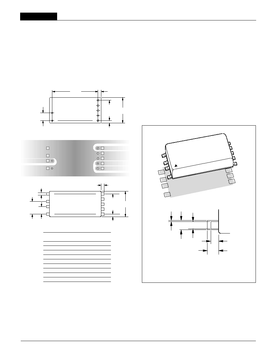
DIMENSIONS IN INCHES (MM)
Case C16A2
Pinout P23
M E C H A N I C A L S P E C I F I C A T I O N S
2.00
(50.80)
4
3
2
1
8
7
6
5
9
0.10
(2.54)
0.110
(2.79)
0.100
(2.54)
0.300
(7.62)
0.500
(12.70)
TOP VIEW
1.00
(25.40)
0.800
(20.32)
4 EQ. SP. @
0.200 (5.08)
0.060
(1.52)
0.055
(1.40)
0.015
(0.38)
0.110
(2.79)
0.015
(0.38)
0.43
(10.92)
DIMENSIONS ARE IN INCHES (MM)
INSULATED BASE
METAL CASE
Case C18
Pinout P25
Performance Specifi cations and Ordering Guide
Output
Input
P A R T N U M B E R S T R U C T U R E
Non-Isolated
Output Confi guration:
U = Unipolar
Nominal Output Voltage:
1.5, 1.8 or 2.5 Volts
Maximum Rated Output
Current in Amps
Input Voltage Range:
D3 = 3.0 to 3.6 Volts (3.3V nominal)
U NR
10
-
/
D3 SM
-
1.8
Packaging:
T = Through-Hole Package
SM = Surface-Mount Package
2
Package
V
OUT
I
OUT
R/N (mVp-p)
Regulation (Max.)
V
IN
Nom. Range I
IN
Effi ciency (Case,
Model (Volts) (Amps) Typ.
Max. Line
Load
(Volts) (Volts) (mA/A) Min.
Typ. Pinout)
UNR-1.5/10-D3T 1.5 10 80
125 ±0.1%
±0.5% 3.3 3.0-3.6 375/5.74 80%
83.5% C16A2, P23
UNR-1.5/10-D3SM 1.5 10 80
125 ±0.1%
±0.5% 3.3 3.0-3.6 375/5.74 80%
83.5% C18, P25
UNR-1.8/10-D3T 1.8 10 80
125 ±0.1%
±0.5% 3.3 3.0-3.6 275/6.38 82.5%
85.5% C16A2, P23
UNR-1.8/10-D3SM 1.8 10 80
125 ±0.1%
±0.5% 3.3 3.0-3.6 275/6.38 83%
85.5% C18, P25
UNR-2.5/10-D3T 2.5 10 80
125 ±0.1%
±0.5% 3.3 3.0-3.6 370/8.51 85%
89% C16A2, P23
UNR-2.5/10-D3SM 2.5 10 80
125 ±0.1%
±0.5% 3.3 3.0-3.6 370/8.51 85%
89% C18, P25
I/O Connections
Pin Function P23 Function P25
1 Logic Ground Logic Ground
2 On/Off Control On/Off Control
3 +Output N.C.
4 Trim N.C.
5 Output Return +Output
6 Input Return Trim
7 +Input Output Return
8 No Pin Input Return
9 No Pin +Input
Typical at T
A
= +25∞C under nominal line voltage and full-load conditions, unless
otherwise noted. All models are tested and specifi ed with an external 470µF input capacitor
with a 20m
ESR and a 6Arms ripple-current rating, as well as a 22µF output capacitor with a
200m
ESR. See I/O Filtering and Noise Reduction for more details.
Ripple/Noise (R/N) is tested/specifi ed over a 20MHz bandwidth. Output noise may be further
reduced by installing additional external output caps. See I/O Filtering and Noise Reduction.
These devices have no minimum-load requirements and will regulate under no-load conditions.
Nominal line voltage, no-load/full-load conditions.
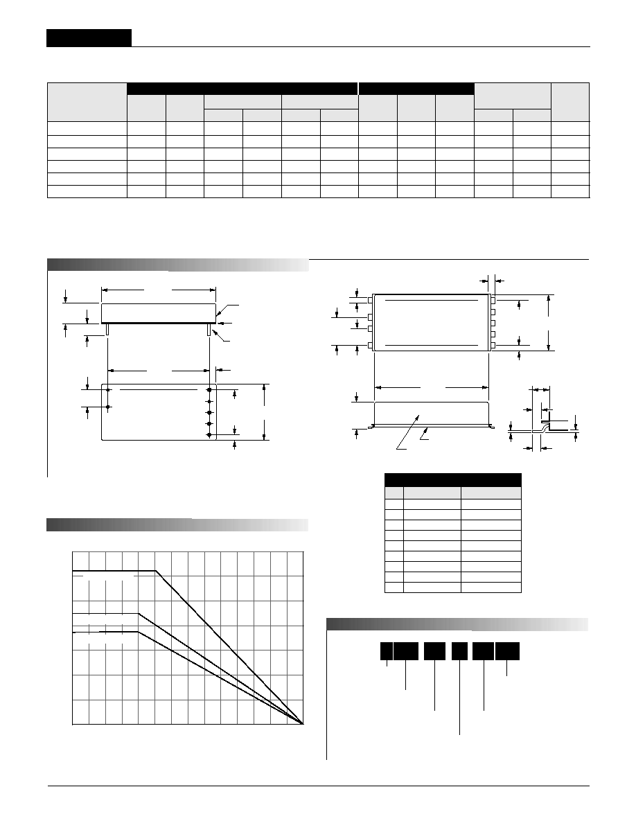
T E M P E R A T U R E D E R A T I N G
O
u
tp
u
t
P
o
w
e
r
(W
a
t
ts
)
Ambient Temperature (
∞
C)
UNR-2.5/10-D3
UNR-1.8/10-D3
UNR-1.5/10-D3
28
24
20
16
12
8
4
0
≠40
0
40
45
50
55
60
65
70
75
80
85
90
95
100
See Temperature Derating section in Technical Notes for more details
.
D3 Models
N O N - I S O L A T E D , 1 5 - 2 5 W , 3 . 3 V - I N P U T D C / D C C O N V E R T E R S
Return Current Paths
These are non-isolated DC/DC converters. The Input Return, Output Return
and Logic Ground pins are all connected together internally. To the extent
possible, all input and load currents should be returned through the Input
Return and Output Return, respectively (via low-impedance runs). Any con-
trol signals applied to the On/Off Control pin should be referenced to Logic
Ground. The internal trace leading to Logic Ground is not designed to carry
high current. Consequently, devices should never be installed in a manner
that results in high current fl ow through Logic Ground (i.e., the Input/Output
Return pins should never be left open or connected via high-impedance paths).
I/O Filtering and Noise Reduction
All UNR 15-25W Series converters are tested and specifi ed with external
470µF input capacitors (20m
ESR, 6Arms ripple-current rating) and exter-
nal 22µF output capacitors (200m
ESR). External input capacitance is
required and must be rated to handle the input ripple current as follows:
In critical applications, input/output ripple/noise may be further reduced by
installing additional I/O caps.
Input
Input Voltage Range 3.0 to 3.6 Volts (3.3V nominal)
Input Current:
Normal Operating Conditions See Ordering Guide
Standby/Off Mode 3.6mA typical, 8mA maximum
Output Short Circuited
500mA typical, 700mA maximum
Input Ripple Current:
UNR-1.5/10-D3, UNR-1.8/10-D3 150mAp-p
UNR-2.5/10-D3 50mAp-p
Input Filter Type Capacitive
Overvoltage Protection None
Reverse-Polarity Protection None
On/Off Control
On = open or 2V to +V
IN
; I
IN
= 800µA max.
Off = 0-0.8V; I
IN
= 1.2mA max.
Output
V
OUT
Accuracy (50% load):
UNR-1.5/10-D3 ±1% (±15mV) maximum
UNR-1.8/10-D3 ±1% (±18mV) maximum
UNR-2.5/10-D3 ±1% (±25mV) maximum
V
OUT
Trim Range
Trim pin tied to +Output:
UNR-1.5/10-D3, UNR-1.8/10-D3 V
OUT
= 1.28 Volts or less
UNR-2.5/10-D3 V
OUT
= 1.52 Volts or less
Trim pin tied to Output Return V
OUT
= 3.0 Volts or greater
Temperature Coeffi cient ±0.02% per ∞C
Ripple/Noise (20MHz BW)
See Ordering Guide
Line/Load Regulation See Ordering Guide
Effi ciency See Ordering Guide
Overcurrent Protection:
Technique "Hiccup" with auto-recovery
Overcurrent Detection Point 140% of rated current
Average Output Current 1 Amp typical, 3 Amps maximum
Dynamic Characteristics
Transient Response (50%-75% step) 25µsec to ±2.5% of fi nal value
Start-Up Time:
V
IN
to V
OUT
25/30msec (1.8/2.5V
OUT
models)
On/Off to V
OUT
25/30msec (1.8/2.5V
OUT
models)
Switching Frequency 300kHz (±30kHz)
Environmental
Operating Temperature (Ambient):
Without Derating ≠40 to +50/55∞C
With Derating to +100∞C (See Derating Curves)
Storage Temperature ≠40 to +105∞C
Physical
Dimensions:
Through-Hole Models 2" x 1" x 0.39" (51 x 25 x 9.9mm)
Surface-Mount Models 2" x 1" x 0.43" (51 x 25 x 10.9mm)
Shielding 5 sided
Case Connection Input/Output Return
Case Material Corrosion-resistant steel with
non-conductive, epoxy-based, black
enamel fi nish and plastic baseplate
Pin Material Copper, tin plated
Weight 1.4 ounces (39.7 grams)
Performance/Functional Specifi cations
Typical @ T
A
= +25∞C under nominal line voltage and full-load conditions unless noted.
All models are tested and specifi ed with an external 470µF input capacitor with a 20m
ESR and a 6Arms ripple-current rating, as well as a 22µF output capacitor with a 200m
ESR.
See I/O Filtering and Noise Reduction for more details. These devices have no minimum-load
requirements and will regulate under no-load conditions. Listed specifi cations apply for both
"T" and "SM" models as appropriate.
See Output Overcurrent Detection for details.
See On/Off Control for details.
See Output Voltage Trimming for details.
For all models, output noise can be further reduced with the installation of additional
external output capacitors. See I/O Filtering and Noise Reduction for details.
Output overcurrent detection initiates at approximately 40% above rated load (14 Amps). Under
overload or short-circuit conditions, output current "hiccups" at approximately 1 Amp average
and remains at that level until the overload is removed. See Output Overcurrent Detection.
See Start-Up Time for details.
See Temperature Derating for details.
Input Voltage:
Continuous 5 Volts
Transient (100msec) 6.3 Volts
Input Reverse-Polarity Protection None
Input/Output Overvoltage Protection None
Output Current Current limited. Devices can
withstand a sustained output
short circuit without damage.
Storage Temperature ≠40 to +105∞C
Lead Temperature (Soldering, 10 sec.) +300∞C
These are stress ratings. Exposure of devices to any of these conditions may adversely
affect long-term reliability. Proper operation under conditions other than those listed in the
Performance/Functional Specifi cations Table is not implied.
Absolute Maximum Ratings
3
T E C H N I C A L N O T E S
I
RMS
= I
OUT
V
OUT
V
IN
V
OUT
V
IN
(
1 ≠
)
r
UNR Series
N O N - I S O L A T E D , 1 5 - 2 5 W , 3 . 3 V - I N P U T D C / D C C O N V E R T E R S
External input capacitors serve primarily as energy-storage elements. They
should be selected for bulk capacitance (at appropriate frequencies), low
ESR, and high rms-ripple-current ratings. The switching nature of modern
DC/DC converters requires that dc input voltage sources have low ac imped-
ance, and highly inductive source impedances can affect system stability.
Your specifi c system confi guration may necessitate additional considerations.
Output ripple/noise (also referred to as periodic and random deviations or
PARD) can be reduced below specifi ed limits using fi ltering techniques, the
simplest of which is the installation of additional external output capacitors.
Output capacitors function as true fi lter elements and should be selected for
bulk capacitance, low ESR, and appropriate frequency response. Any scope
measurements of PARD should be made directly at the DC/DC output pins
with scope probe ground less than 0.5" in length.
All external capacitors should have appropriate voltage ratings and be
located as close to the converters as possible. Temperature variations for all
relevant parameters should be taken into consideration.
The most effective combination of external I/O capacitors will be a function
of your line voltage and source impedance, as well as your particular load
and layout conditions. Our Applications Engineers can recommend potential
solutions and discuss the possibility of our modifying a given device's internal
fi ltering to meet your specifi c requirements. Contact our Applications Engi-
neering Group for additional details.
Input Fusing
UNR 15-25W D3 Series DC/DC converters are not internally fused. Certain
applications and or safety agencies may require the installation of fuses at
the inputs of power conversion components. For DATEL UNR D3 Series
DC/DC converters, you should use either slow-blow or normal-blow fuses
with values no greater than the following.
Output Voltage Fuse Value
1.5V Models 11 Amps
1.8V Models 12 Amps
2.5V Models 18 Amps
Start-Up Time
The V
IN
to V
OUT
Start-Up Time is the interval between the time at which a
ramping input voltage crosses the lower limit of the specifi ed input voltage
range (3.0 Volts) and the fully loaded output voltage enters and remains within
it specifi ed accuracy band. Actual measured times will vary with input source
impedance, external input capacitance, and the slew rate and fi nal value of
the input voltage as it appears to the converter.
The On/Off to V
OUT
Start-Up Time assumes the converter is turned off via
the Remote On/Off Control with the nominal input voltage already applied to
the converter. The specifi cation defi nes the interval between the time at which
the converter is turned on and the fully loaded output voltage enters and
remains within its specifi ed accuracy band. See Typical Performance Curves
for details
Figure 2. Driving the On/Off Control Pin
4
Input Overvoltage and Reverse-Polarity Protection
UNR D3 Series DC/DC converters do not incorporate either input overvoltage
or input reverse-polarity protection. Input voltages in excess of the listed
absolute maximum ratings and input polarity reversals of longer than "instan-
taneous" duration can cause permanent damage to these devices.
+INPUT
LOGIC
GROUND
ON/OFF
CONTROL
1k
Output Overvoltage Protection
UNR D3 Series DC/DC converters do not incorporate output overvoltage
protection. In the extremely rare situation in which the device's feedback loop
is broken, the output voltage may run to excessively high levels (V
OUT
= V
IN
).
If it is absolutely imperative that you protect your load against any and all
possible overvoltage situations, voltage limiting circuitry must be provided
external to the power converter.
Output Overcurrent Detection
Overloading the output of a power converter for an extended period of
time will invariably cause internal component temperatures to exceed their
maximum ratings and eventually lead to component failure. High-current-
carrying components such as inductors, FET's and diodes are at the highest
risk. UNR D3 Series DC/DC converters incorporate an output overcurrent
detection and shutdown function that serves to protect both the power
converter and its load.
Applying an external voltage to the On/Off Control pin when no input power
is applied to the converter can cause permanent damage to the converter.
The on/off control function, however, is designed such that the converter
can be disabled (control pin pulled low) while input power (system 3.3V
power) is ramping up and then "released" once the input has stabilized.
The time duration between the point at which the converter is released and
its fully loaded output settles to within specifi ed accuracy can be found in
the Performance/Functional Specifi cations Table. See Start-Up Time for more
details.
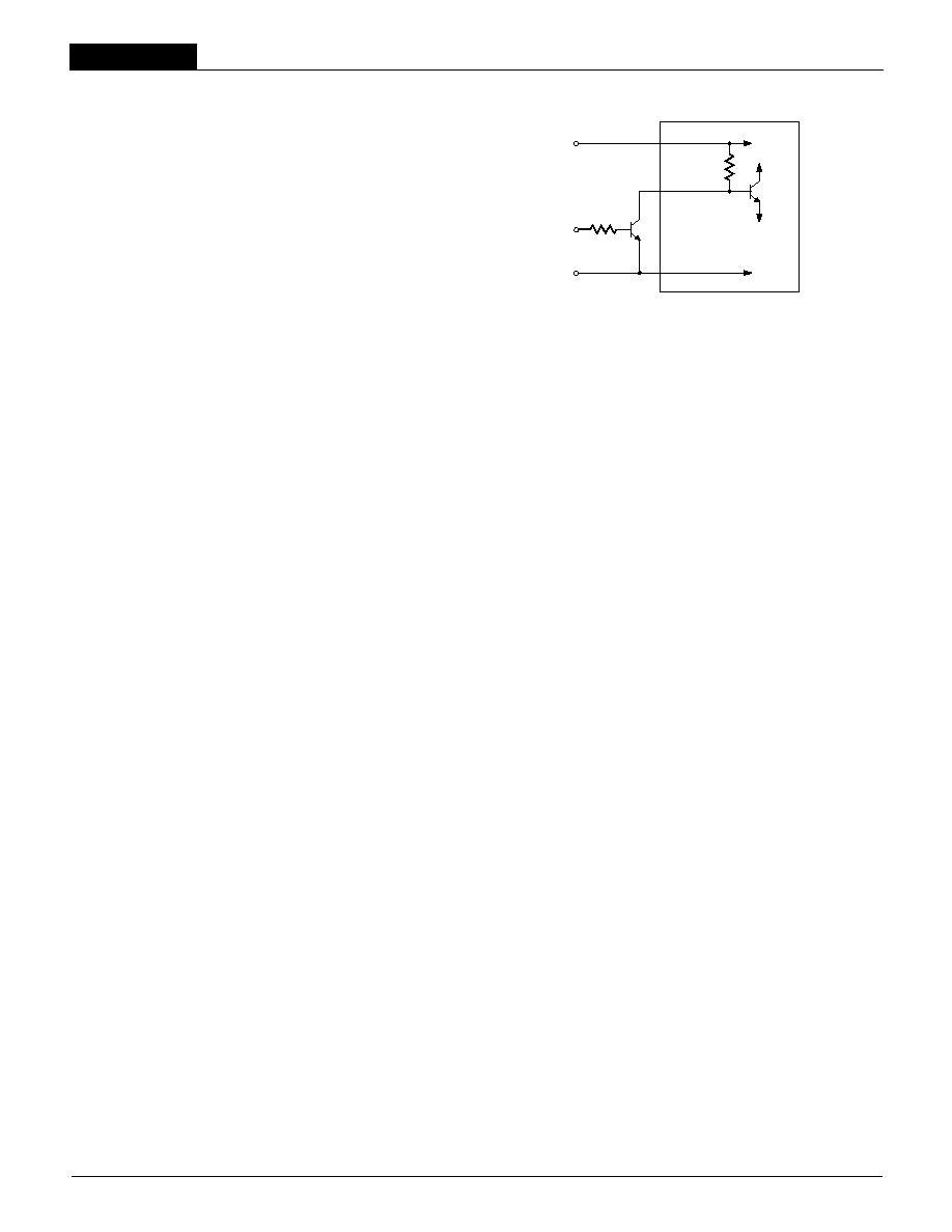
On/Off Control
The On/Off Control pin may be used for remote on/off operation. UNR D3
Series DC/DC converters are designed so that they are enabled when the
control pin is pulled high or left open (normal mode) and disabled when
the control pin is pulled low (to less than +0.8V relative to Logic Ground).
As shown in Figure 2, both 2.5V
OUT
and 1.8V
OUT
models have internal 1k
pull-up resistors to V
IN
(+Input).
Dynamic control of the on/off function is best accomplished with a mechani-
cal relay or open-collector/open-drain drive circuit. The drive circuit should
be able to sink appropriate current when activated and withstand appropriate
voltage when deactivated.
D3 Models
N O N - I S O L A T E D , 1 5 - 2 5 W , 3 . 3 V - I N P U T D C / D C C O N V E R T E R S
5
LOAD
20k
5-10
Turns
+INPUT
INPUT
RETURN
+OUTPUT
TRIM
OUTPUT
RETURN
Trim
Down
Trim Up
LOAD
+INPUT
INPUT
RETURN
+OUTPUT
TRIM
OUTPUT
RETURN
Figure 4. Trim Connections Using Fixed Resistors
Temperature Derating
The outstanding electrical effi ciency of the UNR D3 Series' synchronous-
rectifi er design and the excellent thermal conductivity of its encapsulated
metal package combine to eliminate the need for heat sinking or supplemen-
tal forced-air cooling in the majority of routine applications. As shown in
the derating curves on page 2, 2.5V
OUT
models deliver full rated output
power (25 Watts) up to +55∞C (ambient) and then derate linearly to +100∞C.
1.8V
OUT
models deliver full rated output power (18 Watts) up to +50∞C
(ambient) and similarly derate linearly to +100∞C.
Note: Install either a fi xed trim-up resistor or a fi xed trim-down resistor
depending upon desired output voltage.
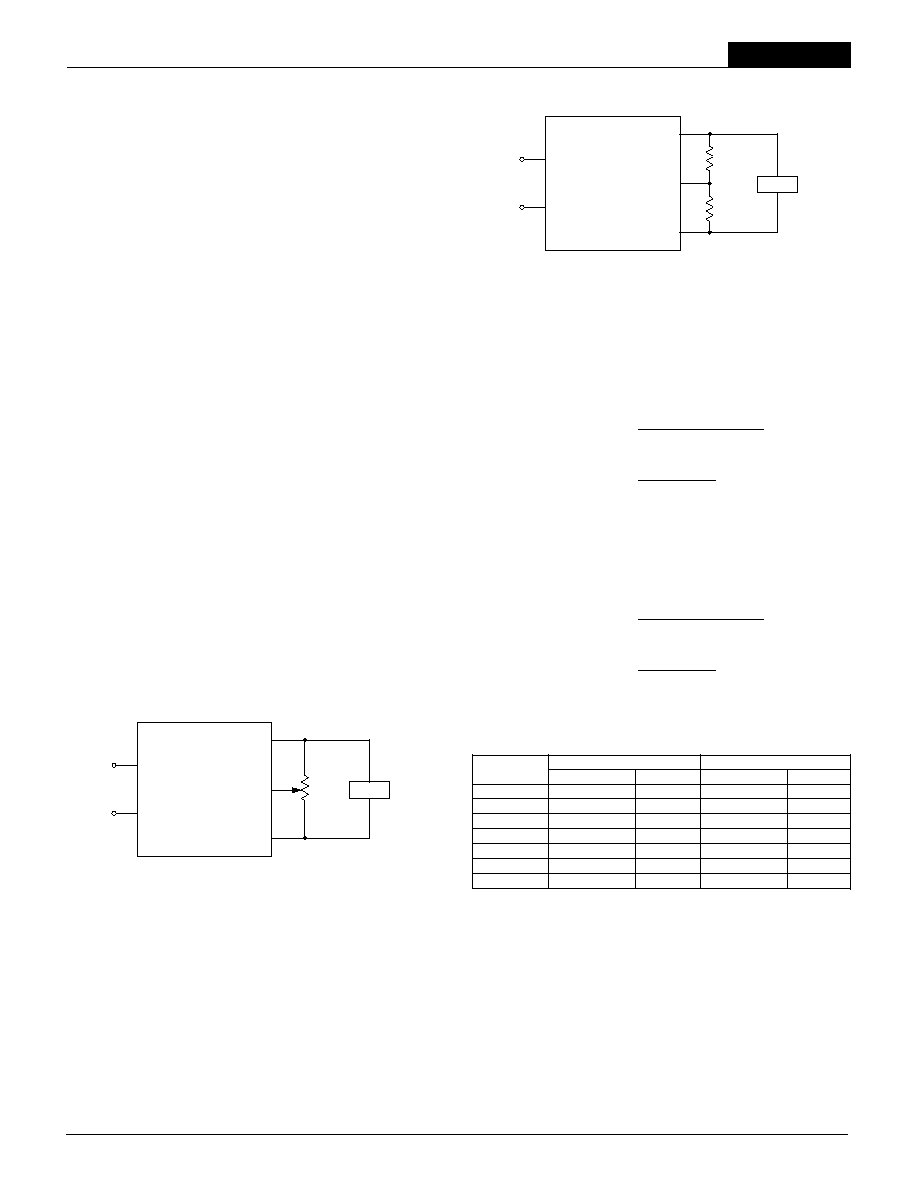
Output Voltage Trimming
For 2.5V
OUT
devices, the output can be trimmed to any voltage between
1.52V and 3.0V. For 1.5V
OUT
and 1.8V
OUT
devices, the output can be trimmed
to any voltage between 1.28V and 3.0V. Trimming is accomplished with either
a trimpot or a single fi xed resistor. The trimpot should be connected between
+Output and Output Return with its wiper connected to the Trim pin as shown
in Figure 3 below.
A trimpot can be used to determine the value of a single fi xed resistor
which should be connected, as shown in Figure 4, between the Trim pin and
+Output to trim down the output voltage, or between the Trim pin and Output
Return to trim up the output voltage. Fixed resistors should be metal-fi lm
types with absolute TCR's less than 100ppm/
∞C to ensure stability.
The equations and look-up table below can be used as starting points for
selecting specifi c trim-resistor values. Recall that untrimmed devices are
guaranteed to be
±1% accurate.
When the output current of a thermally stabilized converter exceeds the maxi-
mum rating (10A) by 40% (typical) to 80% (maximum), the internal overcur-
rent detection circuit automatically shuts down the converter by discharging
the soft-start circuit of the pulse width modulator (PWM). In this off state,
which is similar to that achieved by pulling the On/Off Control low, the output
voltage quickly drops as the output capacitors discharge into the load. Since
there is no longer any output current, the overcurrent detection circuit is
released, allowing the soft-start circuit to recharge and the converter to turn
on again. If the faulty load condition persists, the overcurrent detection circuit
will again discharge the soft-start circuit and shut down the converter. This
continuous on/off cycling of the converter is referred to as "hiccup mode."
Once the overload condition is removed, the converter remains on, and the
output voltage is quickly restored to its regulated value.
The components used to sense the output current have large temperature
coeffi cients. Consequently, in a "cold-start" situation, the Overcurrent Detec-
tion Point may temporarily move to 80% to 120% above the rated current
specifi cation. The device quickly heats up, particularly if an overload situation
exists, and restores the normal (40%) Overcurrent Detection Point. The
device easily survives starting up into an output-short-circuit condition.
The overcurrent detection circuitry helps keep internal current levels and
operating temperatures within safe operating limits. Nevertheless, sustained
operation at current levels above the rated output current (10 Amps) but
below the Overcurrent Detection Point (typically 14 Amps) may result in
permanent damage to the converter (unless active cooling keeps internal
temperatures below safe limits).
Trim-Resistor Equations for 2.5V
OUT
Devices
Trim-Resistor Equations for 1.8V
OUT
Devices
Trim-Resistor Look-Up Table for Common Output Voltages
Desired Output
Voltage (Volts) Trim Resistor (
) Connect To
Trim Resistor (
) Connect To
1.28 0 +Output
N.A.
N.A.
1.52 2.07k +Output
0
+Output
1.8 Open Open
4.03k
+Output
2 16.9k ≠Output
9.35k
+Output
2.5 4.83k ≠Output
Open
Open
2.8 3.38k ≠Output
29.7k
≠Output
3 2.82k ≠Output
17.15k
≠Output
2.5V
OUT
Models
1.8V
OUT
Models
Figure 3. Trim Connections Using a Trimpot
V
OUT
= V
OUT
Desired
R
TRIM
(Ohms) =
7500 (V
OUT
≠1.267)
2.5 ≠ V
OUT
≠1740
R
TRIM
(Ohms) =
Trim Down
Trim Up
V
OUT
≠
2.5
≠1740
9465
V
OUT
= V
OUT
Desired
R
TRIM
(Ohms) =
2670 (V
OUT
≠1.267)
1.8 ≠ V
OUT
R
TRIM
(Ohms) =
V
OUT
≠
1.8
3380
Trim Down
Trim Up
UNR Series
N O N - I S O L A T E D , 1 5 - 2 5 W , 3 . 3 V - I N P U T D C / D C C O N V E R T E R S
6
Recommended PC Board Layout
If necessary, a single pc board layout can accommodate both through-hole
and SMT models of the UNR D3 Series. Note that on page 2 of this data
sheet, the through-hole package is drawn with a bottom view of its pin
locations, and the surface-mount package is drawn with of top view of its
pin locations. As shown below, the through-hole pin locations, when viewed
from above, fall just inside (on 1.8 inch centers) the SMT pin locations (which
essentially begin on 2.1 inch centers). The table below shows how the pin
functions align.
4
3
2
1
8
7
6
5
9
0.10
(2.54)
0.110
(2.79)
0.100
(2.54)
0.300
(7.62)
0.500
(12.70)
TOP VIEW
1.00
(25.40)
0.800
(20.32)
4 EQ. SP. @
0.200 (5.08)
0.10
(2.54)
1
2
3
4
6
7
5
1.800
(45.72)
0.10
(2.54)
0.300
(7.62)
TOP VIEW
1.00
(25.40)
0.800
(20.32)
4 EQ. SP. @
0.200 (5.08)
PINS 1-2, 4: 0.040 ±0.002 (1.016 ±0.051)
PINS 3, 5-7: 0.062 ±0.002 (1.575 ±0.051)
Case C16A2
Case C18
+INPUT
+OUTPUT
ON/OFF CONTROL
TRIM
POWER
GROUND
4 No Pin N.C.
3 No Pin N.C.
2 2 On/Off Control
1 1 Logic Ground
9 7 +Input
8 6 Input Return
7 5 Output Return
6 4 Trim
5 3 +Output
SMT Through-Hole
Pin Number Pin Number Pin Function
Figure 5. Recommended Board Layout
SMT Solder Process for SM models
For the surface-mount "SM" models of the UNR Series, the packages' gull-
wing leads are made of tin-plated (150 microinches) copper. The gull-wing
confi guration, as opposed to "J" leads, was selected to keep the solder joints
out from under the package to minimize both, heat conduction away from the
leads (into the encapsulated package) and shadowing effects.
"SM" modules do not currently withstand the standard solder-refl ow process
with its most common temperature profi les. In order to avoid damage to the
converter a selective solder process (i.e. hot air gun or a hand soldering
method) with the following parameters must therefore be chosen :
Pre-heat phase 30-60∞C rise/minute to 150∞C maximum.
Lead temperature 300∞C for 10 seconds maximum.
As shown in Figure 6, our tests have determined the optimal landing-pad size
to be 160 mils by 130 mils (4 x 3.3 mm).
0.130*
(3.30)
0.015
(0.38)
0.100**
(2.54)
* PAD DIMENSION
** LEAD DIMENSION
0.160*
(4.06)
0.110**
(2.79)
Figure 6 . PC Board Land Pattern

D3 Models
N O N - I S O L A T E D , 1 5 - 2 5 W , 3 . 3 V - I N P U T D C / D C C O N V E R T E R S
T Y P I C A L P E R F O R M A N C E C U R V E S
7
V
IN
to V
OUT
Start-Up Time
On/Off Control to V
OUT
Start-Up Time
UNR-1.8/10-D3 Models
(V
IN
= 3.3V, I
OUT
= 10A, 22µF output capacitor.)
V
OUT
1V/div
V
IN
1V/div
4msec/div
UNR-2.5/10-D3 Models
(V
IN
= 3.3V, I
OUT
= 10A, 22µF output capacitor.)
V
OUT
1V/div
V
IN
1V/div
4msec/div
UNR-1.8/10-D3 Models
(V
IN
= 3.3V, I
OUT
= 10A, 22µF output capacitor.)
V
OUT
1V/div
V
CONTROL
1V/div
4msec/div
UNR-2.5/10-D3 Models
(V
IN
= 3.3V, I
OUT
= 10A, 22µF output capacitor.)
V
OUT
1V/div
V
CONTROL
1V/div
4msec/div

UNR Series
N O N - I S O L A T E D , 1 5 - 2 5 W , 3 . 3 V - I N P U T D C / D C C O N V E R T E R S
DATEL makes no representation that the use of its products in the circuits described herein, or the use of other technical information contained herein, will not infringe upon existing or future patent rights. The descriptions contained herein do not imply the granting of licenses to
make, use, or sell equipment constructed in accordance therewith. Specifi cations are subject to change without notice. The DATEL logo is a registered DATEL, Inc. trademark.
DATEL (UK) LTD. Tadley, England Tel: (01256)-880444
DATEL S.A.R.L. Montigny Le Bretonneux, France Tel: 01-34-60-01-01
DATEL GmbH M¸nchen, Germany Tel: 89-544334-0
DATEL KK Tokyo, Japan Tel: 3-3779-1031, Osaka Tel: 6-354-2025
DATEL, Inc. 11 Cabot Boulevard, Mansfi eld, MA 02048-1151
Tel: (508) 339-3000 (800) 233-2765 Fax: (508) 339-6356
Internet: www.datel.com Email: sales@datel.com
DS-0520A 10/02
INNOVATION and EX C ELL E N C E
Æ
Æ
ISO 9001 REGISTERED
DATEL's world-class design, development and manufacturing team stands
ready to work with you to deliver the exact power converter you need for
your demanding, large volume, OEM applications. And . . . we'll do it on
time and within budget!
Our experienced applications and design staffs; quick-turn prototype capa-
bility; highly automated, SMT assembly facilities; and in-line SPC quality-
control techniques combine to give us the unique ability to design and
deliver any quantity of power converters to the highest standards of quality
and reliability.
We have compiled a large library of DC/DC designs that are currently used
in a variety of datacom/telecom, medical, computer, railway, aerospace and
industrial applications. We may already have the converter you need.
Contact us. Our goal is to provide you the highest-quality, most cost-
effective power converters available.
C U S T O M C A P A B I L I T I E S
90
85
80
75
70
65
60
1
2
3
4
5
6
7
8
9
10
Load Current (Amps)
Efficienc
y (
%
)
V
IN
= 3.0V
V
IN
= 3.6V
V
IN
= 3.3V
UNR-2.5/10-D3 Models
(Guaranteed efficiency = 85% at V
IN
= 3.3V and I
OUT
= 10A)
90
85
80
75
70
65
60
1
2
3
4
5
6
7
8
9
10
Load Current (Amps)
Efficienc
y (
%
)
UNR-1.8/10-D3 Models
(Guaranteed efficiency = 82.5% at V
IN
= 3.3V and I
OUT
= 10A)
V
IN
= 3.6V
V
IN
= 3.3V
V
IN
= 3.0V
Effi ciency vs. Output Current and Input Voltage
T Y P I C A L P E R F O R M A N C E C U R V E S
8
90
85
80
75
70
65
60
1
2
3
4
5
6
7
8
9
10
Load Current (Amps)
Efficienc
y (
%
)
UNR-1.5/10-D3 Models
(Guaranteed efficiency = 80% at V
IN
= 3.3V and I
OUT
= 10A)
V
IN
= 3.6V
V
IN
= 3.3V
V
IN
= 3.0V