unr18-33w_B.indd
DATEL, Inc., Mansfi eld, MA 02048 (USA)
· Tel: (508)339-3000, (800)233-2765 Fax: (508)339-6356 · Email: sales@datel.com · Internet: www.datel.com
Single Output
UNR D5/D12 Series
Features
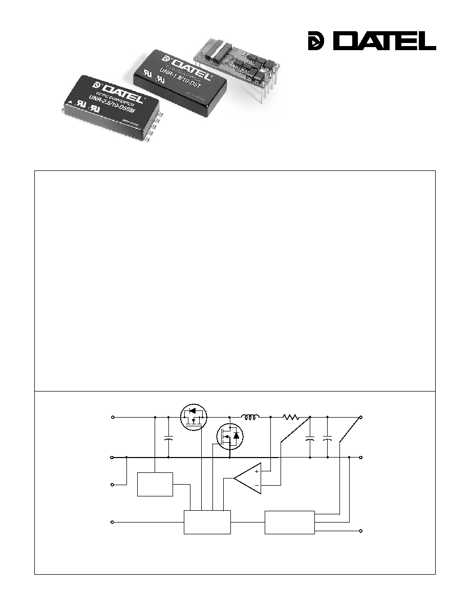
Figure 1. Simplifi ed Schematic
INNOVATION and EX C ELL E N C E
®
®
As supply voltages trend lower and load currents increase, centralized power
becomes more impractical. The tight accuracy, low noise and quick transient
response demanded by today's low voltage CPU's, ASIC's and DSP's make power
processing at the point of use the only viable solution. The UNR 18-33W series
provides a complete line of non-isolated DC/DC converters to satisfy this require-
ment. With input voltages of 5V (-D5 models) and 12V (-D12 models) these convert-
ers offer standard output voltages of 1.8, 2.5 and 3.3 Volts and up to 10 Amps of
output current in both through-hole and surface-mount 1" x 2" metal cases.
With on/off control and output voltage trim capability as standard features, these
non-isolated converters exploit full synchronous rectifi cation, planar magnetics, and
100% automated assembly to deliver high effi ciencies (to 91%) and low noise at
low cost.
These versatile DC/DC's are fully line and load regulated. They feature quick
transient response (50µsec), user-optional on/off control (for power sequencing),
and output overcurrent detection and shutdown ("hiccup" technique with auto-
recovery). Their impressive guaranteed effi ciencies enable them to deliver fully rated
output power from 40 to +50/55°C (ambient) without supplemental cooling.
If your high current requirements have made the use of ineffi cient linear regula-
tors impractical, take a look at one of DATEL's new switching buck regulators. Their
high effi ciency, ease-of-use, long-term reliability, and overall cost effectiveness will
impress you. Safety agency approvals and EMC characterizations are currently in
progress.
+V
IN
+V
OUT
INPUT
RETURN
LOGIC
GROUND
ON/OFF
CONTROL
PWM
CONTROLLER
VOLTAGE
BOOST
REFERENCE &
ERROR AMP
OVERCURRENT
DETECTION
OUTPUT
RETURN
V
OUT
TRIM
+V
CC
Non-Isolated, 5 or 12V
IN
to 1.8/2.5/3.3V
OUT
8 and 10 Amp DC/DC Converters
Input ranges of 4.75-5.5V or 10.8-13.6V
Output voltages of 1.8/2.5/3.3V
8 and 10 Amp output current models
V
OUT
user-trimmable from 1.28V to 3.6V
Non-isolated, full synchronous topology
1" x 2" through-hole or SMT package
Gull-wing leads/standard refl ow for SMT
High effi ciency to 91%; Low noise
200kHz switching; Planar magnetics
40 to +40/50/60°C ambient operation with
no derating
Remote on/off control; Output overcurrent
detection
IEC950/EN60950/UL1950 approval
!
!
!
!
!
!
!
!
!
!
!
!
-D5 models only.
UNR Series
N O N - I S O L A T E D , 1 8 - 3 3 W , 5 & 1 2 V - I N P U T D C / D C C O N V E R T E R S
M E C H A N I C A L S P E C I F I C A T I O N S
2.00
(50.80)
4
3
2
1
8
7
6
5
9
0.10
(2.54)
0.110
(2.79)
0.100
(2.54)
0.300
(7.62)
0.500
(12.70)
TOP VIEW
1.00
(25.40)
0.800
(20.32)
4 EQ. SP. @
0.200 (5.08)
0.060
(1.52)
0.055
(1.40)
0.015
(0.38)
0.110
(2.79)
0.015
(0.38)
0.43
(10.92)
DIMENSIONS ARE IN INCHES (MM)
INSULATED BASE
METAL CASE
Case C18
Performance Specifi cations and Ordering Guide
Output
Input
Non-Isolated
Output Confi guration:
U = Unipolar
Nominal Output Voltage:
1.8, 2.5 or 3.3 Volts
Maximum Rated Output
Current in Amps
Input Voltage Range:
D5 = 4.75 to 5.5 Volts (5V nominal)
D12 = 10.8 to 13.6 Volts (12V nominal)
U NR
10
-
/
D5 SM
-
1.8
Packaging:
T
= Through-Hole Package
SM
= Surface-Mount Package
2
Package
V
OUT
I
OUT
R/N (mVp-p)
Regulation (Max.)
V
IN
Nom. Range I
IN
Effi ciency (Case,
Model (Volts) (Amps) Typ.
Max. Line
Load
(Volts) (Volts) (mA/mA) Min.
Typ. Pinout)
UNR-1.8/10-D5T 1.8 10 70
100 ±0.1%
±0.5% 5 4.75-5.5 150/4190 82%
86% C16A2, P23
UNR-1.8/10-D5SM 1.8 10 40
80 ±0.1%
±0.5% 5 4.75-5.5 150/4190 82%
86% C18, P25
UNR-2.5/10-D5T 2.5 10 75
100 ±0.1%
±0.5% 5 4.75-5.5 150/5620 85%
89% C16A2, P23
UNR-2.5/10-D5SM 2.5 10 75
100 ±0.1%
±0.5% 5 4.75-5.5 150/5620 85%
89% C18, P25
UNR-3.3/8-D5T 3.3 8 40
80 ±0.1%
±0.5% 5 4.75-5.5 100/5470 88%
92% C16A1, P23
UNR-3.3/8-D5SM 3.3 8 40
80 ±0.1%
±0.5% 5 4.75-5.5 100/5470 88%
92% C18, P25
UNR-3.3/8-D12T 3.3 8 40
100 ±0.25%
±0.875% 12 10.8-13.6 50/2420 86%
91% C16A1, P23
UNR-3.3/8-D12SM 3.3 8 40
100 ±0.25%
±0.875% 12 10.8-13.6 50/2420 86%
91% C18, P25
UNR-3.3/10-D5T 3.3 10 40
80 ±0.1%
±0.5% 5 4.75-5.5 150/7250 86%
91% C16A2, P23
UNR-3.3/10-D5SM 3.3 10 50
100 ±0.1%
±0.5% 5 4.75-5.5 150/7250 86%
91% C18, P25
UNR-3.3/10-D12T 3.3 10 70
120 ±0.25%
±0.875% 12 10.8-13.6 90/3090 86%
89% C16C2, P23
UNR-3.3/10-D12SM 3.3 10 70
120 ±0.25%
±0.875% 12 10.8-13.6 90/3090 86%
89% C18, P25
I/O Connections
Pin Function P23 Function P25
1 Logic Ground Logic Ground
2 On/Off Control On/Off Control
3 +Output N.C.
4 Trim N.C.
5 Output Return +Output
6 Input Return Trim
7 +Input Output Return
8 No Pin Input Return
9 No Pin +Input
Typical at T
A
= +25°C under nominal line voltage and full-load conditions, unless
otherwise noted. All models are tested and specifi ed with an external 22µF output capacitor
with a 200m
ESR and a 470µF input capacitor with 6Arms ripple-current rating and 20m
ESR. See I/O Filtering and Noise Reduction for more details.
Ripple/Noise (R/N) is tested/specifi ed over a 20MHz bandwidth. Output noise may be further
reduced by installing additional external output caps. See I/O Filtering and Noise Reduction.
These devices have no minimum-load requirements and will regulate under no-load conditions.
Nominal line voltage, no-load/full-load conditions.
0.10
(2.54)
METAL CASE
2.00
(50.80)
0.20 MIN
(5.08)
SEE
NOTES
INSULATED BASE
1
2
3
4
6
7
5
1.800
(45.72)
0.10
(2.54)
0.300
(7.62)
BOTTOM VIEW
DIMENSIONS IN INCHES (MM)
1.00
(25.40)
0.800
(20.32)
4 EQ. SP. @
0.200 (5.08)
0.10
(2.54)
CASE C16A1
CASE HEIGHT:
0.39 (9.91)
PIN DIAMETERS:
PINS 1-7:
0.040 ±0.002 (1.016 ±0.051)
CASE C16A2
CASE HEIGHT:
0.39 (9.91)
PIN DIAMETERS:
PINS 1-2, 4:
0.040 ±0.002 (1.016 ±0.051)
PINS 3, 5-7:
0.062 ±0.002 (1.575 ±0.051)
CASE C16C2
CASE HEIGHT:
0.48 (12.19)
PIN DIAMETERS:
PINS 1-2, 4:
0.040 ±0.002 (1.016 ±0.051)
PINS 3, 5-7:
0.062 ±0.002 (1.575 ±0.051)
Case C16A1, A2,C2
P A R T N U M E R S T R U C T U R E
UNR Models
N O N - I S O L A T E D , 1 8 - 3 3 W , 5 & 1 2 V - I N P U T D C / D C C O N V E R T E R S
Return Current Paths
These are non-isolated DC/DC converters. The Input Return, Output Return
and Logic Ground pins are all connected together internally. To the extent
possible, all input and load currents should be returned through the Input
Return and Output Return, respectively (via low-impedance runs). Any con-
trol signals applied to the On/Off Control pin should be referenced to Logic
Ground. The internal trace leading to Logic Ground is not designed to carry
high current. Consequently, devices should never be installed in a manner
that results in high current fl ow through Logic Ground (i.e., the Input/Output
Return pins should never be left open or connected via high-impedance paths).
I/O Filtering and Noise Reduction
All UNR 18-33W Series converters are tested and specifi ed with external
470µF input capacitors (20m
ESR, 6Arms ripple-current rating) and exter-
nal 22µF output capacitors (200m
ESR). External input capacitance is
required and must be rated to handle the input ripple current as follows:
In critical applications, input/output ripple/noise may be further reduced by
installing additional I/O caps.
Input
Input Voltage Range 3.0 to 3.6 Volts (3.3V nominal)
D5 Models 4.75-5.5 Volts (5V nominal)
D12 Models 10.8-13.6 Volts (12V nominal)
Input Current:
Normal Operating Conditions See Ordering Guide
Standby/Off Mode 3.6mA typical
Input Ripple Current:
1.8/2.5V Models 150mAp-p
3.3/8 -D5 Models 100mAp-p
3.3/10 -D5 Models 150mAp-p
3.3/8 -D12 Models 110mAp-p
3/3/10 -D12 Models 250mAp-p
Input Filter Type Capacitive
Overvoltage Protection None
Reverse-Polarity Protection None
On/Off Control:
Functionality TTL high (or open) = on, low = off
Logic Threshold +0.8-2.0 Volts (1.5V typical)
Output
V
OUT
Accuracy (50% load):
1.8V
OUT
Models ±2% of V
OUT
maximum
2.5/3.3V
OUT
Models ±1% of V
OUT
maximum
V
OUT
Trim Range
Trim pin tied to +Output: V
OUT
= 1.52 Volts or less
Trim pin tied to Output Return V
OUT
= 3.6 Volts or greater
Temperature Coeffi cient ±0.02% per °C
Ripple/Noise (20MHz BW)
See Ordering Guide
Line/Load Regulation See Ordering Guide
Effi ciency See Ordering Guide
Overcurrent Protection:
Technique "Hiccup" with auto-recovery
Overcurrent Detection Point 110-180% of rated current
Average Short Circuit Current:
D5 Models 1 Amp typical, 3 Amps maximum
D12 Models 4 Amp typical, 6 Amps maximum
Dynamic Characteristics
Transient Response (50-100% load):
1.8/2.5V
OUT
Models 60µsec to 2.5% of fi nal value
3.3V
OUT
-D5 Models 50µsec to 2.5% of fi nal value
3.3/8 -D12 Models 50µsec to 1% of fi nal value
3.3/10 -D12 Models 50µsec to 2.5% of fi nal value
Start-Up Time:
V
IN
to V
OUT
25/30msec (1.8/2.5V
OUT
models)
On/Off
to
V
OUT
25/30msec (1.8/2.5V
OUT
models)
Switching Frequency 300kHz (±30kHz)
Environmental
Operating Temperature (Ambient):
Without Derating See Derating Curves
With Derating to +100°C (See Derating Curves)
Storage Temperature 40 to +105°C
Physical
Dimensions:
D5 Through-Hole Models 2" x 1" x 0.39" (51 x 25 x 9.9mm)
D5 Surface-Mount Models 2" x 1" x 0.43" (51 x 25 x 10.9mm)
D12 Through-Hole Models 2" x 1" x 0.48" (51 x 25 x 12.2mm)
D12 Surface-Mount Models 2" x 1" x TBD" (51 x 25 x 12.7mm)
Performance/Functional Specifi cations
Typical @ T
A
= +25°C under nominal line voltage and full-load conditions unless noted.
All models are tested and specifi ed with an external 470µF input capacitor with a 20m
ESR and a 6Arms ripple-current rating, as well as a 22µF output capacitor with a 200m
ESR.
See I/O Filtering and Noise Reduction for more details. These devices have no minimum-load
requirements and will regulate under no-load conditions. Listed specifi cations apply for both
"T" and "SM" models as appropriate.
See Output Overcurrent Detection for details.
See On/Off Control for details.
See Output Voltage Trimming for details.
For all models, output noise can be further reduced with the installation of additional
external output capacitors. See I/O Filtering and Noise Reduction for details.
See Start-Up Time for details.
See Temperature Derating for details.
Input Voltage:
Continuous:
D5 Models 7 Volts
D12 Models 15 Volts
Transient (100msec) 15 Volts
Input Reverse-Polarity Protection None
Input/Output Overvoltage Protection None
Output Current Current limited. Devices can
withstand a sustained output
short circuit without damage.
Storage Temperature 40 to +105°C
Lead Temperature (Soldering, 10 sec.) +300°C
These are stress ratings. Exposure of devices to any of these conditions may adversely
affect long-term reliability. Proper operation under conditions other than those listed in the
Performance/Functional Specifi cations Table is not implied.
Absolute Maximum Ratings
3
T E C H N I C A L N O T E S
Physical
Shielding 5 sided
Case Connection Input/Output Return
Case Material Corrosion-resistant steel with
non-conductive, epoxy-based, black
enamel fi nish and plastic baseplate
Pin Material Copper, tin plated
I
RMS
= I
OUT
V
OUT
V
IN
V
OUT
V
IN
(
1
)
r
UNR Series
N O N - I S O L A T E D , 1 8 - 3 3 W , 5 & 1 2 V - I N P U T D C / D C C O N V E R T E R S
External input capacitors serve primarily as energy-storage elements. They
should be selected for bulk capacitance (at appropriate frequencies), low
ESR, and high rms-ripple-current ratings. Input capacitors compensate for
I·R drops on input lines and power sources. Providing a solid input voltage
will greatly reduce the need for capacitors. The switching nature of modern
DC/DC converters requires that dc input voltage sources have low ac imped-
ance, as highly inductive source impedances can affect system stability. Your
specifi c system confi guration may necessitate additional considerations.
Output ripple/noise (also referred to as periodic and random deviations or
PARD) can be reduced below published specifi cations by using fi ltering
techniques, the simplest of which is the installation of additional external
output capacitors. Output capacitors function as true fi lter elements and
should be selected for bulk capacitance, low ESR, and appropriate frequency
response. Any scope measurements of PARD should be made directly at the
DC/DC output pins with scope probe ground less than 0.5" in length.
All external capacitors should have appropriate voltage ratings and be
located as close to the converters as possible. Temperature variations for all
relevant parameters should be taken into consideration.
The most effective combination of external I/O capacitors will be a function
of your line voltage and source impedance, as well as your particular load
and layout conditions. Our Applications Engineers can recommend potential
solutions and discuss the possibility of our modifying a given device's internal
fi ltering to meet your specifi c requirements. Contact our Applications Engi-
neering Group for additional details.
Input Fusing
UNR 18-33W Series converters are not internally fused. Certain applications
and or safety agencies may require the installation of fuses at the inputs of
power conversion components. Fuses should also be used if the possibility
of sustained, non-current-limited, input-voltage polarity reversals exists. For
DATEL UNR 18-33W Series DC/DC converters, you should use either slow-
blow or normal-blow fuses with values no greater than the following.
Output Voltage
Fuse Value
1.8V Models
9 Amps
2.5V Models
12 Amps
3.3/8-D5 Models 12.5 Amps
3.3/10-D5 Models 16 Amps
3.3/8-D12 Models 6 Amps
3.3/10-D12 Models 7 Amps
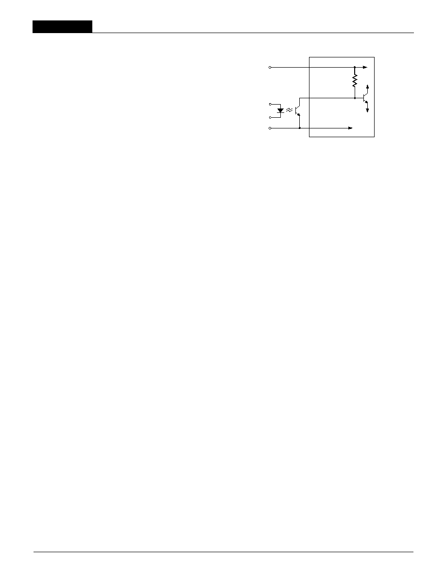
Figure 2. Driving the On/Off Control Pin
4
Input Overvoltage and Reverse-Polarity Protection
UNR 18-33W Series DC/DC converters do not incorporate either input over-
voltage or input reverse-polarity protection. Input voltages in excess of the
listed absolute maximum ratings and input polarity reversals of longer than
"instantaneous" duration can cause permanent damage to these devices.
+INPUT
LOGIC
GROUND
ON/OFF
CONTROL
R
PULL UP
D5 Models 4.99k
D12 Models 12.4k
Dynamic control of the on/off function is best accomplished with a mechanical
relay or open-collector/open-drain drive circuit (optically isolated if appropri-
ate). The drive circuit should be able to sink appropriate current when
activated and withstand appropriate voltage when deactivated.
Applying an external voltage to the On/Off Control pin when no input power is
applied to the converter can cause permanent damage to the converter. The
on/off control function, however, is designed such that the converter can
be disabled (control pin pulled low) while input voltage is ramping up and
then "released" once the input has stabilized. The time duration between the
point at which the converter is released and its fully loaded output settles
to within specifi ed accuracy can be found in the Performance/Functional
Specifi cations Table. See Start-Up Time for more details.
Start-Up Time
The V
IN
to V
OUT
Start-Up Time is the interval between the time at which a
ramping input voltage crosses the lower limit of the specifi ed input voltage
range (4.75V for D5 models, 10.8V for D12 models) and the fully loaded
output voltage enters and remains within it specifi ed accuracy band. Actual
measured times will vary with heavy capacitive loading.
The On/Off to V
OUT
Start-Up Time assumes the converter is turned off via
the Remote On/Off Control with the nominal input voltage already applied
to the converter. The specifi cation defi nes the interval between the time at
which the converter is turned on and the fully loaded output voltage enters
and remains within its specifi ed accuracy band. See Typical Performance
Curves for details
Output Overvoltage Protection
UNR 18-33W Series DC/DC converters do not incorporate output overvolt-
age protection. In the extremely rare situation in which the device's feedback
loop is broken, the output voltage may run to excessively high levels. If it is
absolutely imperative that you protect your load against any and all possible
overvoltage situations, voltage limiting circuitry must be provided external to
the power converter.
Output Overcurrent Detection
Overloading the output of a power converter for an extended period of
time will invariably cause internal component temperatures to exceed their
maximum ratings and eventually lead to component failure. High-current-
carrying components such as transformers, FET's and diodes are at the
highest risk. UNR 18-33W Series DC/DC converters incorporate an output
overcurrent detection and shutdown function that serves to protect both the
power converter and its load.
On/Off Control
The On/Off Control pin may be used for remote on/off operation. UNR
18-33W Series DC/DC converters are designed so that they are enabled
when the control pin is pulled high or left open (normal mode) and disabled
when the control pin is pulled low (to less than +0.8V relative to Logic
Ground). As shown in Figure 2, D5 models have internal 4.99k
pull-up
resistors to V
IN
(+Input), while D12 models have 12.4k
.
UNR Models
N O N - I S O L A T E D , 1 8 - 3 3 W , 5 & 1 2 V - I N P U T D C / D C C O N V E R T E R S
Output Voltage Trimming
UNR 18-33W devices can be trimmed to any voltage between 1.52V and
3.6V. Trimming is accomplished with either a trimpot or a single fi xed resistor.
The trimpot should be connected between +Output and Output Return with
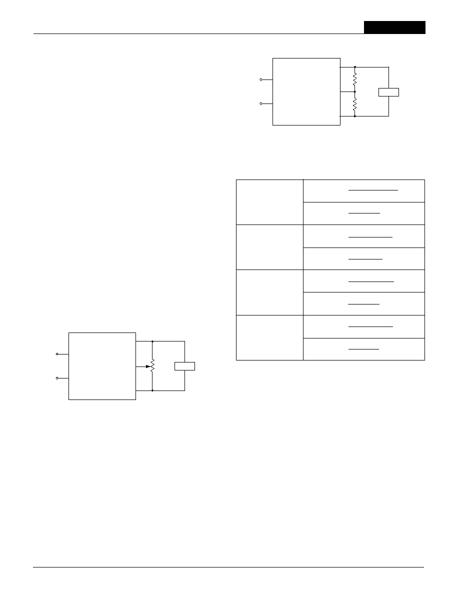
its wiper connected to the Trim pin as shown in Figure 3 below.
A trimpot can be used to determine the value of a single fi xed resistor
which should be connected, as shown in Figure 4, between the Trim pin and
+Output to trim down the output voltage, or between the Trim pin and Output
Return to trim up the output voltage. Fixed resistors should be metal-fi lm
types with absolute TCR's less than 100ppm/
°C to ensure stability.
The equations below can be used as starting points for selecting specifi c
trim-resistor values. Recall that untrimmed devices are guaranteed to be
between
±1% and ±2% accurate, depending on model. See Performance
and Functional Specifi cations.
5
LOAD
20k
5-10
Turns
+INPUT
INPUT
RETURN
+OUTPUT
TRIM
OUTPUT
RETURN
Trim
Down
Trim Up
LOAD
+INPUT
INPUT
RETURN
+OUTPUT
TRIM
OUTPUT
RETURN
Figure 4. Trim Connections Using Fixed Resistors
Note: Install either a fi xed trim-up resistor or a fi xed trim-down resistor
depending upon desired output voltage.
When the output current of a thermally stabilized converter exceeds the
maximum rating by 40% (typical) to 80% (maximum), the internal overcurrent
detection circuit shuts down the converter by discharging the soft-start circuit
of the pulse width modulator (PWM). In this off state, which is similar to that
achieved by pulling the On/Off Control low, the output voltage quickly drops
as the output capacitors discharge into the load. Since there is no longer any
output current, the overcurrent detection circuit is released, allowing the soft-
start circuit to recharge and the converter to turn on again. If the faulty load
condition persists, the overcurrent detection circuit will again discharge the
soft-start circuit and shut down the converter. This continuous on/off cycling
of the converter is referred to as "hiccup mode." Once the overload condition
is removed, the converter remains on, and the output voltage is quickly
restored to its regulated value.
The components used to sense the output current have large temperature
coeffi cients. Consequently, in a "cold-start" situation, the Overcurrent Detec-
tion Point may temporarily move to 80% to 120% above the rated current
specifi cation. The device quickly heats up, particularly if an overload situation
exists, and restores the normal (40%) Overcurrent Detection Point. The
device will not be damaged by starting up into an output-short-circuit condition.
The overcurrent detection circuitry helps keep internal current levels and
operating temperatures within safe operating limits. Nevertheless, sustained
operation at current levels above the rated output current but below the Over-
current Detection Point may result in permanent damage to the converter.
Figure 3. Trim Connections Using a Trimpot
UNR-1.8/10-D5T
UNR-1.8/10-D5SM
UNR-2.5/10-D5T
UNR-2.5/10-D5SM
1.74
UP
R
T
(k
) =
V
O
1.8
3.14
1.74
DOWN
R
T
(k
) =
2.5 V
O
7.5(V
O
1.26)
1.74
UP
R
T
(k
) =
V
O
2.5
9.47
1.0
DOWN
R
T
(k
) =
3.3 V
O
7.5(V
O
1.27)
UNR-3.3/8-D5T
UNR-3.3/8-D5SM
UNR-3.3/10-D5T
UNR-3.3/10-D5SM
UNR-3.3/8-D12T
UNR-3.3/8-D12SM
UNR-3.3/10-D12T
UNR-3.3/10-D12SM
1.0
UP
R
T
(k
) =
V
O
3.3
9.5
1.0
DOWN
R
T
(k
) =
3.3 V
O
7.5(V
O
1.26)
1.0
UP
R
T
(k
) =
V
O
3.3
9.41
1.74
DOWN
R
T
(k
) =
1.8 V
O
2.49(V
O
1.26)
Note: Resistor values are in k
. Accuracy of adjustment is subject to
tolerances of resistors and factory-adjusted output accuracy.
V
O
= desired output voltage.