Äîêóìåíòàöèÿ è îïèñàíèÿ www.docs.chipfind.ru
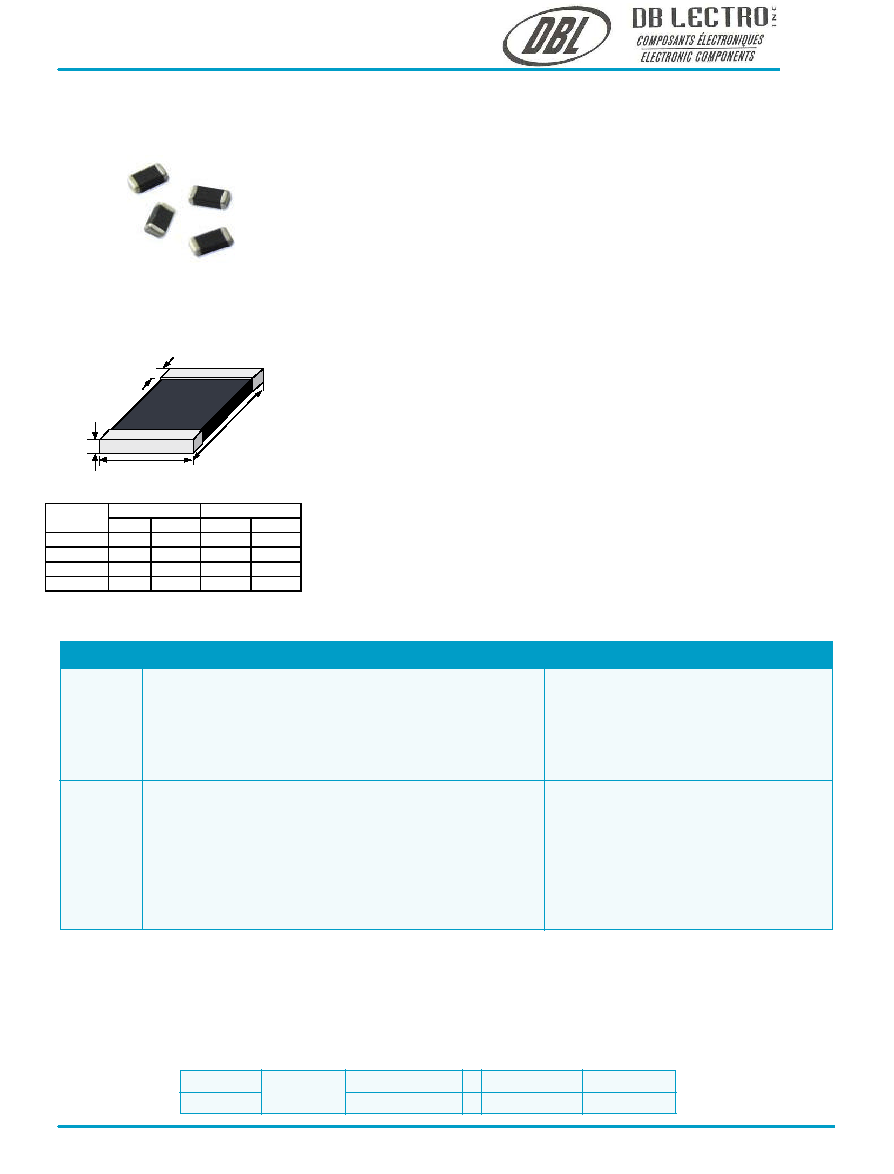
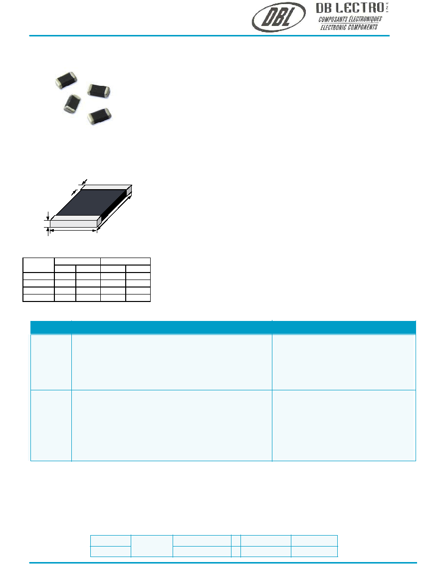
INCHES
MILLIMETERS
SYMBOL
MIN
MAX
MIN
MAX
T
-
0.047
-
1.20
a
0.006
0.026
0.15
0.65
L
0.071
0.087
1.80
2.20
W
0.043
0.055
1.10 1.40
V
A R I S T O RS
TVS 0805 SMD
Multilayer Ceramic Transient
Voltage Suppressor
Standard Capacity
Specifications
P a c k a g i n g
Tape and Reel
T
7 inch reel (3.000 pcs.)
M a t e r i al
Dimensions
T
a
W
L
Features
Thin layer, high precise techniques
Lead free
Bi-directional clamping
Standard capacity
Available with Nickel/Tin end termination
Applications
Circuit board and ESD, EFT
Protection of:
·
I/O ports
·
Keyboards
·
LCD`s
·
Sensors
Body:
Ceramic (ZnO)
Terminals:
Ni/Sn plated (code "P")
Ag/Pt/Pd non plated
(code "N" on request)
Operating Te m p e r a t u r e
-55 to +125°C
Solderability
acc. to IEC 60068-2-58
235°C, 2s
Soldering Heat Resistanc e
260ºC, 10 sec. (IEC 60068-2-58)
280ºC, 5 sec. (IEC 60068-2-58)
Response Time
<0.5ns
Temperatur e
coefficient (
V) of
clamping
voltage (Vc) @ specified test current
<0.01%/°C
Power dissipation
0.1W max.
S t a n d a r ds
IEC 61000-4-2
MIL-STD-883C
Maximum Ratings (125°C)
Specifications (25°C)
Type
max. cont.
working
voltage
max.
non-repetitive
surge current
max. non-repetitive
surge energy
(10/1000
µs)
max. clamping
voltage at spec.
current
nominal voltage
at 1mA (DC)
test current
typ.
capacitance
typ.
inductance
(V)
(V)
(A)
(J)
(V@A)
(V)
(V)
(pF)
(pF)
(nH)
JV0805ML030A
JV0805ML050A
JV0805ML090A
JV0805ML120A
JV0805ML140A
JV0805ML180A
JV0805ML220A
JV0805ML260A
JV0805ML300A
JV0805ML680A
3,3
5,5
9,0
12,0
14,0
18,0
22,0
26,0
30,0
68,0
2,5
4,0
6,0
9,0
11,0
14,0
17,0
20,0
25,0
50,0
60
100
120
120
120
120
120
120
100
80
0,30
0,30
0,30
0,30
0,30
0,30
0,30
0,30
0,30
0,30
10,0 @ 5
15,5 @ 5
23,0 @ 5
25,0 @ 5
30,0 @ 5
40,0 @ 5
44,0 @ 5
58,0 @ 5
65,0 @ 5
135,0 @ 5
3,8
7,1
10,0
14,0
16,0
22,0
24,3
29,5
35,0
74,0
7,0
9,8
14,5
18,5
21,0
28,0
30,0
38,0
43,0
90,0
4200
1950
1580
1110
1230
760
735
460
330
95
4000
1700
1340
950
1050
690
620
420
290
85
1,5
1,5
1,5
1,5
1,5
1,5
1,5
1,5
1,5
1,5
Specifications are subjec t
to change without notice
Orde r Qty.
Order-
Type
Terminal Code Packaging
Information
Numbe r
JV 0805ML180
A
P
T
V
M ( A C )
V
M ( D C )
I
T M
W
T M
V
C
V
N ( D C ) m i n .
V
N ( D C ) m a x .
C
t y p .
C
t y p .
L
t y p .
(8/20
µs)
(8/20
µs)
1KHz
.
1MHz
.
DB LECTRO Inc. 3600 boul. Matte suite i Brossard Qc J4Y-2Z2 tel:(450)-444-1424 fax:(450)-444-4714 www.dblectro.com
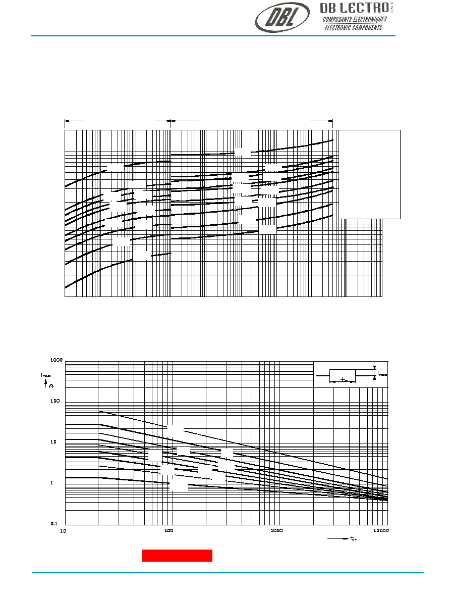
JV0805ML030A
CURRENT (I)
MAXIMUM CLAMPING VOLTAGE (V)
1
10
100
Maximum Leakage
Maximum Clamping Voltage
1
µ
A
10
µ
A
1 0 A
1 0 m A
100
µ
A
1 m A
1 0 0 m A
1 A
100A
1000A
s
t
m a x
i
= f ( , p u l s e t r a i n )
r
M a x i m u m s u r g e c u r r e n t
V
A R I S T O RS
TVS 0805 SMD
Maximum Surge Current:
V/I C h a r a c t e r i s t i cs
JV0805ML6 80A
JV0805ML3 00A
JV0805ML260A
JV0805ML220A
JV0805ML180A
JV0805ML140A
JV0805ML120A
JV0805ML090A
JV0805ML050A
JV0805ML0 30A
22,0
14,0
12,0
9,0
3,3
30,0
26,0
18,0
5,5
68,0
22,0
14,0
12,0
9,0
3,3
30,0
26,0
18,0
5,5
68,0
1
x
2
10
10
2
10
3
10
5
10
6
10
4
Maximum surge current i
m a x
=f(t
r
,pulse train)
DB LECTRO Inc. 3600 boul. Matte suite i Brossard Qc J4Y-2Z2 tel:(450)-444-1424 fax:(450)-444-4714 www.dblectro.com
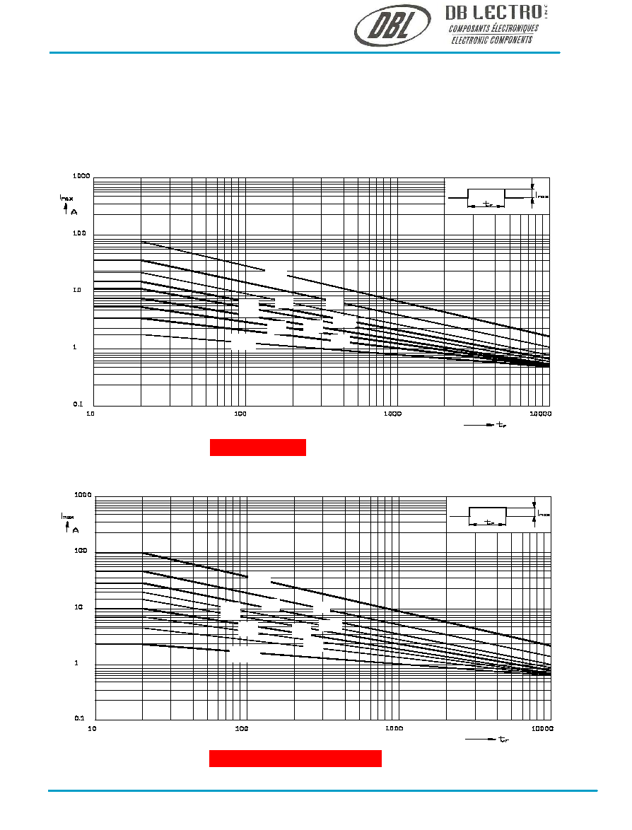
JV0805ML680A
JV0805ML050A, JV0805ML300A
s
t
m a x
i
= f ( , p u l s e t r a i n )
r
M a x i m u m s u r g e c u r r e n t
s
t
m a x
i
= f ( , p u l s e t r a i n )
r
M a x i m u m s u r g e c u r r e n t
V
A R I S T O RS
Maximum Surge Current:
TVS 0805 SMD
Maximum Surge Current:
1
x
2
10
10
2
10
3
10
5
10
6
10
4
1
x
2
10
10
2
10
3
10
5
10
6
10
4
Maximum surge current i
m a x
=f(t
r
,pulse train)
Maximum surge current i
m a x
=f(t
r
,pulse train)
DB LECTRO Inc. 3600 boul. Matte suite i Brossard Qc J4Y-2Z2 tel:(450)-444-1424 fax:(450)-444-4714 www.dblectro.com
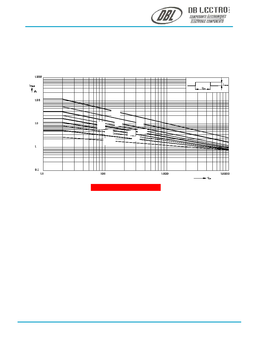
JV0805ML090A- JV0805ML260A
M a x i m u m s u r g e c u r r e n t
s
= f ( , p u l s e t r a i n )
i
t
m a x
r
V
A R I S T O RS
TVS 0805 SMD
Maximum Surge Current:
1
x
2
10
10
2
10
3
10
5
10
6
10
4
Maximum surge current i
m a x
=f(t
r
,pulse train)
DB LECTRO Inc. 3600 boul. Matte suite i Brossard Qc J4Y-2Z2 tel:(450)-444-1424 fax:(450)-444-4714 www.dblectro.com
INCHES
MILLIMETERS
SYMBOL
MIN
MAX
MIN
MAX
T
-
0.047
-
1.20
a
0.006
0.026
0.15
0.65
L
0.071
0.087
1.80
2.20
W
0.043
0.055
1.10 1.40
V
ARISTORS
TVS 0805SMD
Multilayer Ceramic Transient
Voltage Suppressor
Low Capacity
Specifications
P a c k a g i n g
Tape and Reel
T
7 inch reel (3.000 pcs.)
M a t e r i al
Dimensions
T
a
W
L
Features
Thin layer, high precise techniques
Lead free
Bi-directional clamping
low capacity
Available with Nickel/tin end terminatio n
Applications
Circuit board and ESD, EFT
Protection of:
·
I/O ports
·
Keyboards
·
LCD`s
·
Sensors
Body:
Ceramic (ZnO)
Terminals:
Ni/Sn plated (code "P")
Ag/Pt/Pd non plated
(code "N" on request)
Operating Te m p e r a t u r e
-55 to +125°C
Solderability
acc. to IEC 60068-2-58
235°C, 2s
Soldering Heat Resistanc e
260ºC, 10 sec. (IEC 60068-2-58)
280ºC, 5 sec. (IEC 60068-2-58)
Response Time
<0.5ns
Temperatur e
coefficient (
V) of
clamping
voltage (Vc) @ specified test current
<0.01%/°C
Power dissipation
0.1W max.
S t a n d a r ds
IEC 61000-4-2
MIL-STD-883C
Maximum Ratings (125°C)
Specifications (25°C)
JV0805ML030L
JV0805ML050L
JV0805ML090L
JV0805ML120L
JV0805ML140L
JV0805ML180L
JV0805ML220L
JV0805ML260L
JV0805ML300L
3,3
5,5
9,0
12,0
14,0
18,0
22,0
26,0
30,0
2,5
4,0
6,0
9,0
11,0
14,0
17,0
20,0
25,0
40
40
40
40
40
40
40
40
40
0,10
0,10
0,10
0,10
0,10
0,10
0,10
0,10
0,10
10,0@ 2
15,5 @ 2
23,0 @ 2
25,0 @ 2
30,0 @ 2
40,0 @ 2
44,0 @ 2
58,0 @ 2
65,0 @ 2
3,8
7,1
10,0
14,0
16,0
22,0
24,3
29,5
35,0
7,0
9,8
14,5
18,5
21,0
28,0
30,0
38,0
43,0
208 0
790
650
560
445
330
320
330
220
190 0
720
550
480
380
290
280
285
190
1,5
1,5
1,5
1,5
1,5
1,5
1,5
1,5
1,5
Specifications are subject
to change without notice
Orde r Qty.
Order-
Type
Terminal Code Packaging
Information
Numbe r
JV 0805ML140
L
P
T
Type
max. cont.
working
voltage
max.
non-repetitive
surge current
max. non-repetitive
surge energy
(10/1000
µs)
max. clamping
voltage at spec.
current
nominal voltage
at 1mA (DC)
test current
typ.
capacitance
typ.
inductance
(8/20
µs)
(8/20
µs)
1KHz
.
1MHz
.
V
M ( A C )
(V)
(V)
V
M ( D C )
(nH)
(pF)
(pF)
(V)
(V)
(V@A)
(J)
(A)
I
T M
W
T M
V
C
V
N ( D C ) m i n .
V
N ( D C ) m a x .
C
t y p .
C
t y p .
L
t y p .
DB LECTRO Inc. 3600 boul. Matte suite i Boul. Matte suite i Brossard Qc J4Y-2Z2 tel:(450)-444-1424 fax:(450)-444-4714 www.dblectro.com