 | ÐлекÑÑоннÑй компоненÑ: JV08CH270 | СкаÑаÑÑ:  PDF PDF  ZIP ZIP |
Äîêóìåíòàöèÿ è îïèñàíèÿ www.docs.chipfind.ru
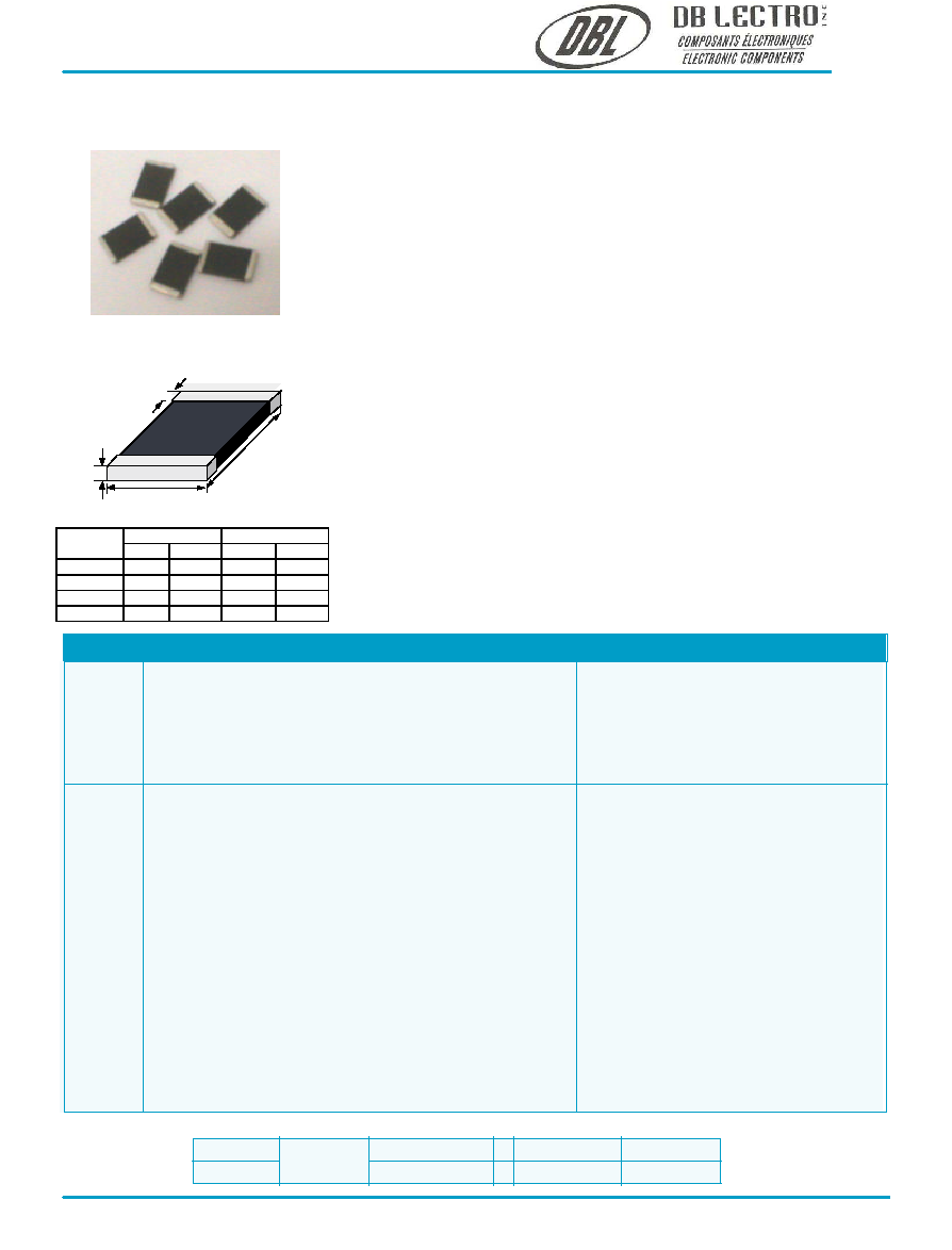
INCHES
MILLIMETERS
SYMBOL
MIN
MAX
MIN
MAX
T
-
0.080
-
2.03
a
0.016
0.050
0.41
1.27
L
0.311
0.335
7.90
8.51
W
0.185
0.207
4.70 5.26
V
ARISTORS
JV 08CH SMD
Surface Mount
Metal Oxide Varistors
Specifications
Packaging
Tape and Reel
Standard:
13 inch reel (4.000 pcs.)
Option: 7 inch reel (1.000 pcs.)
Material
Dimensions
T
a
W
L
Features
Monolayer Construction in a 5mm x 8mm
Package Size.
Leadless, Surface chip form
Bi-directional clamping
No derating up to 125°C ambient.
Available with Nickel/Tin end termination
Applications
·
Surface-mount chip form intended for
hybrid-circuit application
·
PCs and peripherals
·
Utility meters
·
Proximity switches
·
Consumer products
·
Protection of various kinds of
transistors
diodes
ICs
thyristors
triacs and
·
semiconductors...etc.,
Body:
Ceramic (ZnO)
Terminals:
Ni/Sn plated (code "P")
Operating Temperature
-55 to +125°C
Solderability
acc. to IEC 60068-2-58
235°C, 2s
Soldering Heat Resistanc e
260ºC, 10 sec. (IEC 60068-2-58)
280ºC, 5 sec. (IEC 60068-2-58)
Response Time
<0.5ns
Temperature
coefficient (
V) of
clamping
voltage (Vc) @ specified test current
<0.01%/°C
Power dissipation
0.25W max.
Maximum Ratings (125°C )
Specifications (25°C )
JV08CH180
JV08CH220
JV08CH270
JV08CH330
JV08CH390
JV08CH470
JV08CH560
JV08CH680
JV08CH820
JV08CH101
JV08CH121
JV08CH151
JV08CH181
JV08CH201
JV08CH221
JV08CH241
JV08CH271
JV08CH331
JV08CH361
JV08CH391
JV08CH431
14,0
18,0
22,0
26,0
31,0
38,0
45,0
56,0
65,0
85,0
102
127
153
175
180
200
220
270
300
330
369
11,0
14,0
17,0
20,0
25,0
30,0
35,0
40,0
50,0
65,0
75,0
95,0
115
130
140
150
180
200
230
250
275
250
250
250
250
250
250
250
250
500
500
500
500
500
500
500
500
500
500
500
500
500
0,80
0,80
1,00
1,20
1,50
1,80
2,30
3,00
4,20
4,80
6,00
8,00
10,0
11,0
12,0
13,0
14,0
16,0
20,0
21,0
23,0
36,0 @ 5
46,0 @ 5
54,0 @ 5
67,0 @ 5
75,0 @ 5
89,0 @ 5
106 @ 5
135 @ 5
135 @ 10
165 @ 10
197 @ 10
250 @ 10
290 @ 10
340 @ 10
356 @ 10
389 @ 10
437 @ 10
520 @ 10
593 @ 10
647 @ 10
705 @ 10
16,0
18,7
23,0
30,0
35,0
42,0
50,0
62,0
74,0
90,0
108
135
162
184
198
216
245
300
324
351
387
20,0
26,0
31,0
36,0
43,0
52,0
62,0
74,0
90,0
110
132
165
198
228
242
268
270
330
396
429
473
3805
1835
1590
1250
1050
970
838
800
625
565
340
270
230
200
180
165
130
110
110
100
100
3100
1600
1350
1070
900
820
710
680
530
480
300
250
200
180
160
150
120
100
100
90
90
3,0
3,0
3,0
3,0
3,0
3,0
3,0
3,0
3,0
3,0
3,0
3,0
3,0
3,0
3,0
3,0
3,0
3,0
3,0
3,0
3,0
Specifications are subject
to change without notice
Type
max. cont.
working
voltage
max.
non-repetitive
surge current
max. non-repetitive
surge energy
(10/1000
µs)
max. clamping
voltage at spec.
current
nominal voltage
at 1mA (DC)
test current
typ.
capacitance
typ.
inductance
(8/20
µs)
(8/20
µs)
1KHz
.
1MHz
.
V
M(AC)
(V)
(V)
V
M(DC)
(nH)
(pF)
(pF)
(V)
(V)
(V@A)
(J)
(A)
I
TM
W
TM
V
C
V
N(DC)min.
V
N(DC)max.
C
typ.
C
typ.
L
typ.
Orde r Qty.
Order-
Type
Terminal Code Packaging
Information
Number
JV 08CH361
P
T
DB LECTRO Inc. 3600 boul. Matte suite i Brossard Qc J4Y-2Z2 tel:(450)-444-1424 fax:(450)-444-4714 www.dblectro.com
JV08CH820- JV08CH431
500
400
300
200
100
9 0
8 0
7 0
6 0
5 0
4 0
3 0
2 0
1000A
100A
10A
1A
100mA
1 0 m A
1mA
1 0
PEAK AMPERES (A)
MAXIMUM PEAK VOLTAGE (V)
MAXIMUM CLAMPING VOLTAGE
MODEL SIZE 5 x 8 mm
TA=-55TO125
JV08CH680
JV08CH560
JV08CH470
JV08CH390
JV08CH330
JV08CH270
JV08CH220
JV08CH180
Transient V/I Characteristics Curves:
JV08CH180- JV08CH680
JV 08CH SMD
V
ARISTORS
5000
4000
3000
2000
1000
900
800
700
600
500
400
300
200
10000A
1000A
100A
10A
1A
100mA
10mA
1mA
100
PEAK AMPERES (A)
MAXIMUM PEAK VOLTAGE (V)
MAXIMUM CLAMPING VOLTAGE
MODEL SIZE 5 x 8 mm
TA=-55TO125
Transient V/I Characteristics Curves:
JV08CH431
JV08CH391
JV08CH361
JV08CH331
JV08CH271
JV08CH241
JV08CH221
JV08CH201
JV08CH181
JV08CH151
JV08CH121
JV08CH101
JV08CH820
DB LECTRO Inc. 3600 boul. Matte suite i Brossard Qc J4Y-2Z2 tel:(450)-444-1424 fax:(450)-444-4714 www.dblectro.com
JV08CH180- JV08CH680
JV08CH820- JV08CH431
I M P U L S E D U R A T I O N
s)
(
1 0 0 0 0
1 0 0 0
SURGE CURRENT (A)
2 0
100
1
1 0
100
5 0 0
2 0 0
5 0
20
5
2
1 0 0 0
2 0 0 0
1 0 0
2 0
1
10
1 0 0
5 0 0
1 0 0 0
1 0 0 0 0
(
s )
2 0 0
50
20
5
2
0 . 5
0 . 2
SURGE CURRENT (A)
I M P U L S E D U R A T I O N
V
ARISTORS
JV 08CH SMD
Pulse Rating Curves:
Pulse Rating Curves:
MODEL SIZE 5 x 8 mm
JV08CH180-JV08CH680
MODEL SIZE 5 x 8 mm
JV08CH820-JV08CH431
10
1
2
10
2
10
3
10
4
10
5
10
6
INDEFINITE
10
4
10
5
10
6
INDEFINITE
10
3
10
2
1
2
10
DB LECTRO Inc. 3600 boul. Matte suite i Brossard Qc J4Y-2Z2 tel:(450)-444-1424 fax:(450)-444-4714 www.dblectro.com
Absolute Maximum Ratings
Continuous: CH SERIES UNITS
Steady State Applied Voltage:
AC Voltage Range (V
M(AC)RMS
) ... ... ... ... ... ... ... ... ... ... ... ... ... ... ... ... ... ... ... ... ... ... ... . 11 to 275 V
DC Voltage Range (V
M(DC)
) ... ... ... ... ... ... ... ... ... ... ... ... ... ... ... ... ... ... ... ... ... ... ... ... .. 14 to 369 V
Transient:
Peak Pulse Current (I
TM
)
For 8/20µs Current Wave (See Figure2) ... ... ... ... ... ... ... ... ... ... .... ... ... ... ... ... ... ... .. 250 to 500 A
Single Pulse Energy Range
For 10/1000µs Current Wave (W
TM
) ... ... ... ... ... ... ... ... ... ... ... ... ... ... ... ... ... ... ... ... .. 0.8 to 23 J
Operating Ambient Temperature Range(T
A
) ... ... ... ... ... ... ... ... ... ... ... ... ... ... ... ... ... . -55 to 125
Storage Temperature Range (T
STG
) ... ... ... ... ... ... ... ... ... ... ... ... ... ... ... ... ... ... ... ... ... -55 to 150
Temperature Coefficient (av) of Clamping Voltage (V
C
) at Specified Test Current ... .
0.01
/
Standard Shipping Quantities
Tape and reel is the standard packaging method of the CH series. There are 1,000 pcs /reel/7 inch.
Less than 100 pieces sample quantity, the units are shipped bulk pack.
Recommended Pad Outline
SYMBOL
INCHES
MILLIMETERS
A
0.402
10.21
B
0.216
5.50
C
0.087
2.21
A
B
C
Note
NoteAvoid metal runs in this area
V
ARISTORS
JV 08CH SMD
DB LECTRO Inc. 3600 boul. Matte suite i Brossard Qc J4Y-2Z2 tel:(450)-444-1424 fax:(450)-444-4714 www.dblectro.com
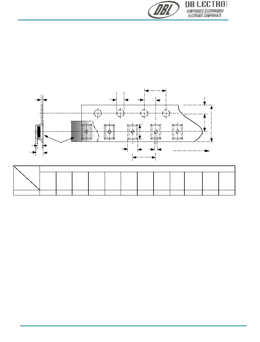
Tape and Reel Specifications
Embossed Taping
Tape in accordance can be supplied to IEC publication 286-3
DIMENSIONS (mm)
Symbol
Type
A
0
±0.1
B
0
±0.1
W
±0.3
F
±0.1
E
±0.1
P
1
±0.1
P
2
±0.1
P
0
±0.1
D
0
0.1
0
T
Max.
T
2
Max.
D
1
Min.
08CH
5.5
8.5
16
7.5
1.75
8.0
2.0
4.0
1.5
1.0
3.0
1.5
K
0
Depth of Cavity: Dependent Chip Size to Minimize Rotation
Precautions to the user for CH-series Surface mount MOV:
1. Soldering recommendation:
Material: 62/36/2 Sn/Pb/Ag or equivalent
Reflow temperature/time: 230 max. /10 sec. max.
Flux: non-activated
2. When mounting surface mount varistor on the PC board, the improper soldering temperature and time
out of the limits may reduce the adhesive strength of their terminals.
3. Put the proper volume of solderthe height of filleton PC board for installing surface mount
varistors, because it directly affects the installed varistors. The design of copper pad patterns and
dimensions should be set, so that the proper volume of solder can provide.
4. Do not use solvents such as thinner and acetone, which dissolve or make the exterior covering of
varistor deteriorate. Ultrasonic cleaning shall be so set that the vibration can not travel the assembly
boards.
5. For surface mount CH series MOV, use flux with a halogen content of less than 0.2 wt. Do not use
strong acid flux.
6. Store varistors at temperature of 10 to +40 and relative humidity of less than 75. Avoid storing
in environment of rapid changes in temperature, direct sunlight, corrosive, gas or dust, and store with
the varistors packaged.
A
0
P
1
D
1
B
0
D
0
P
0
P
2
E
W
F
Top Tape
Direction of unreeling
T
K
0
T
2
JV 08CH SMD
V
ARISTORS
DB LECTRO Inc. 3600 boul. Matte suite i Brossard Qc J4Y-2Z2 tel:(450)-444-1424 fax:(450)-444-4714 www.dblectro.com