
3 19
Contents
1.Module Classification Information
2.Precautions in use of LCD Modules
3.General Specification
4.Absolute Maximum Ratings
5.Electrical Characteristics
6.Optical Characteristics
7.Interface Pin Function
8.Contour Drawing & Block Diagram
9.Function Description
10.Character Generator ROM Pattern
11.Instruction Table
12.Timing Characteristics
13.Initializing of LCM
14.Quality Assurance
15.Reliability
www.dblectro.com
4 19
1.Module Classification Information
W P 1 6 0 2 B
Y JCS
,
6
BrandDB LECTRO Inc.
Display TypeH Character Type, G Graphic Type , P PLED
Display FontCharacter 16 words, 2Lines.
Model serials no.
Backlight Type Y Yellow Green
ErrSpecial Code
JCS: English and Japanese standard font
2.Precautions in use of PLED Modules
(1)Avoid applying excessive shocks to the module or making any alterations or modifications to
it.
(2)Don't make extra holes on the printed circuit board, modify its shape or change the
components of PLED module.
(3)Don't disassemble the PLEDM.
(4)Don't operate it above the absolute maximum rating.
(5)Don't drop, bend or twist PLEDM.
(6)Soldering: only to the I/O terminals.
(7)Storage: please storage in anti-static electricity container and clean environment.
3.General Specification
Item Dimension
Unit
Number of Characters
16 characters x 2 Lines
Module dimension
80.0 x 36.0 x 9.7(MAX)
mm
View area
66.0 x 16.0
mm
Active area
50.67 x 10.36
mm
Dot size
0.51 x 0.60
mm
Dot pitch
0.54 x 0.63
mm
Character size
2.67 x 5.01
mm
Character pitch
3.20 x 5.35
mm
LCD type
PLED , Green
www.dblectro.com

5 19
Duty 1/16
4.Absolute Maximum Ratings
Item Symbol
Min
Typ
Max
Unit
Operating Temperature
T
OP
-20
25
+50
Storage Temperature
T
ST
-30
+70
Input Voltage
V
I
-0.3
V
DD
V
Supply Voltage For Logic
V
DD
-V
SS
-0.3
7 V
Supply Voltage For LCD
V
BT-
V
SS
-0.3
5.0 V
5.Electrical Characteristics
Item Symbol
Condition
Min
Typ
Max
Unit
Supply Voltage For Logic
V
DD
-V
SS
4.5 5.0 5.5 V
Supply Voltage For LCD
V
BT
Ta=25
2.0 2.5 5.0 V
Input High Volt.
V
IH
0.7 V
DD
V
DD
V
Input Low Volt.
V
IL
-0.3
0.55 V
Output High Volt.
V
OH
2.4
V
Output Low Volt.
V
OL
0.4 V
Supply Current
I
DD
V
DD
=5V
0.35 0.6 mA
6.Optical Characteristics
Item Symbol
Condition
Min
Typ
Max
Unit
www.dblectro.com
6 19
(V)
80 deg
View Angle
(H)
80 deg
Contrast Ratio
CR
100 lux
100
T rise
10 us
Response Time
T fall
10 us
Brightness
With
polarizer
40 nits
7.Interface Pin Function
Pin No. Symbol
Level
Description
1 V
SS
0V
Ground
2 V
DD
5.0V
Supply Voltage for logic
3
V
BT
(Variable) Operating voltage for PLED Brightness adjhstment
4
RS
H/L
H: DATA, L: Instruction code
5 R/W H/L
H: Read(MPU
Module) L: Write(MPU Module)
6 E
H,H
L Chip enable signal
7
DB0
H/L
Data bit 0
8
DB1
H/L
Data bit 1
9
DB2
H/L
Data bit 2
10
DB3
H/L
Data bit 3
11
DB4
H/L
Data bit 4
12
DB5
H/L
Data bit 5
13
DB6
H/L
Data bit 6
14
DB7
H/L
Data bit 7
15 NC
16 NC
www.dblectro.com

7 19
Brightness Control
VBT Brightness(nits) Power
consumption(measured with random texts)
2.5V 20(typical)
50mW
3.0V 45(typical)
63mW
Note:1.When random texts pattern is running,averagely,at any instance,about 1/4 of pixels will be
on.
2.If VBT is not operated within 2V and 3V,non-uniformity display may occur.
3.You have to use the saving mode by VBT 2.5V in order to make long life.
8.Contour Drawing &Block Diagram
www.dblectro.com

8 19
00
40
01
41
02
42
03
43
04
44
05
45
06
46
07
47
08
48
09
49
0A
4A
0B
4B
0C
4C
0D
4D
0E
4E
0F
4F
3
1 2
4 5 6 7 8 9 10
14
12
11
13
16
15
Character located
DDRAM address
DDRAM address
MPU
80 series
RS
R/W
E
DB0~DB7
or
68 series
Controller/Com Driver
16X2 LCD
Com1~16
Seg1~40
D
Seg Driver
M
CL1
CL2
Seg41~80
Vdd,Vss,Vbt
Bias and P
o
w
e
r Circ
uit
Vdd
Vbt
Vss
4.6
75.0
2.5
40.55
80.0 0.5
36
.
0
0.5
5.7
10
.3
13.12
31.0
2.
5
18
.3
4.95
7.55
15.21
8.0
P2.54*15=38.1
1.8
16- 1.0PTH
2
9.7Max
4.9
1.6
4- 2.5 PTH
4- 5.0 PAD
25
.
2
16
.
0
(
V
A
)
10
.3
6(
A
A
)
71.2
64.0(VA)
50.67(AA)
Vss
RS
R/W
Vo
DB2
DB0
DB1
E
Vdd
9
7
8
6
2
4
5
3
1
DB6
DB4
DB5
NC
NC
DB7
13
16
15
14
11
12
10
DB3
0.34
0.53
0.51
0.54
2.67
0.6
0.63
5.
0
1
DOT SIZES
1
16
www.dblectro.com

9 19
9.Function Description
The LCD display Module is built in a LSI controller, the controller has two 8-bit registers, an
instruction register (IR) and a data register (DR).
The IR stores instruction codes, such as display clear and cursor shift, and address information
for display data RAM (DDRAM) and character generator (CGRAM). The IR can only be written
from the MPU. The DR temporarily stores data to be written or read from DDRAM or
CGRAM. When address information is written into the IR, then data is stored into the DR from
DDRAM or CGRAM. By the register selector (RS) signal, these two registers can be selected.
RS R/W
Operation
0
0
IR write as an internal operation (display clear, etc.)
0
1
Read busy flag (DB7) and address counter (DB0 to DB7)
1
0
Write data to DDRAM or CGRAM (DR to DDRAM or CGRAM)
1
1
Read data from DDRAM or CGRAM (DDRAM or CGRAM to DR)
Busy Flag (BF)
When the busy flag is 1, the controller LSI is in the internal operation mode, and the next
instruction will not be accepted. When RS=0 and R/W=1, the busy flag is output to DB7. The
next instruction must be written after ensuring that the busy flag is 0.
Address Counter (AC)
The address counter (AC) assigns addresses to both DDRAM and CGRAM
Display Data RAM (DDRAM)
This DDRAM is used to store the display data represented in 8-bit character codes. Its extended
capacity is 80
�8 bits or 80 characters. Below figure is the relationships between DDRAM
addresses and positions on the liquid crystal display.
AC
(hexadecimal)
High bits
Low bits
AC6 AC5 AC4 AC3 AC2 AC1 AC0
1 0 0 1 1 1 0
Example: DDRAM addresses 4E
www.dblectro.com

10 19
Character Generator ROM (CGROM)
The CGROM generate 5
�8 dot or 5�10 dot character patterns from 8-bit character codes. See
Table 2.
Character Generator RAM (CGRAM)
In CGRAM, the user can rewrite character by program. For 5
�8 dots, eight character patterns
can be written, and for 5
�10 dots, four character patterns can be written.
Write into DDRAM the character code at the addresses shown as the left column of table 1. To
show the character patterns stored in CGRAM.
Display position DDRAM address
00 01 02 03 04 05 06 07 08 09 0A 0B 0C 0D 0E 0F
40 41 42 43 44 45 46 47 48 49 4A 4B 4C 4D 4E 4F
2-Line by 16-Character Display
1 2 3 4 5 6 7 8 9 10 11 12 13 14 15 16
www.dblectro.com

11 19
Relationship between CGRAM Addresses, Character Codes (DDRAM) and Character
patterns
Table 1.
F o r 5 * 8 d o t c h a r a c t e r p a t t e r n s
C h a r a c t e r C o d e s
( D D R A M d a t a )
C G R A M A d d r e s s
C h a r a c t e r P a t t e r n s
( C G R A M d a t a )
5
4 3 2
1 0
6
7
5
4 3 2
0
1
7 6 5
4 3 2
1 0
0 0 0
0
0
1
1
0
0
1
0
1
0
1
0
0
1
1
1
1
0
1
1
1
0
0
0
0
0
1
1
0
0
1
0
1
0
1
0
0
1
1
1
1
0
1
1
1
0
0
0
0
0
1
0
1
0
0
1
1
1
1
0
1
1
1
* * *
* * *
* * *
* * *
* * *
* * *
* * *
* * * 0 0 0 0 0
* * *
* * *
* * *
* * *
* * *
* * *
* * *
* * * 0 0 0 0 0
0 0
0 0
0 0
0 0
0 0
0 0
0
0
0
0 0 0
0 0 0
0 0
0
0
0 0
0
0 0 0
0 0 0
0
0 0 0
0
0
1
* * *
* * *
1 1 1
0 0 0 0
* 1 1 1
0 0 0 0
* 0 0 0
0 0 0 0
* 0 0
1
H i g h L o w
H i g h L o w
H i g h L o w
F o r 5 * 1 0 d o t c h a r a c t e r p a t t e r n s
C h a r a c t e r C o d e s
( D D R A M d a t a )
C G R A M A d d r e s s
C h a r a c t e r P a t t e r n s
( C G R A M d a t a )
7
H i g h L o w
4
5
6
3 2
1 0
H i g h L o w
5
4 3 2
1 0
H i g h L o w
7 6 5
4
1
2
3
0
* * * 0 0 0 0 0
0 0 0 0 0
* * *
* * *
* * *
* * *
* * *
* * *
* * *
* * *
* * *
* * *
* * * * * * * *
0 0 0 0
0 0 0
1
0 0
1 0
0 0
1 1
0
1 0 0
0
1 0
1
0
1 1 0
0
1 1 1
1 0 0 0
1 0 0
1
1 0
1 0
1 1 1 1
0 0 0 0 0
0 0 0 0
* 0 0 0
0 0
0
0
0 0
0 0 0
0 0 0
0
0 0 0 0
0 0 0 0
0 0 0 0
C h a r a c t e r
p a t t e r n ( 1 )
C u r s o r p a t t e r n
C h a r a c t e r
p a t t e r n ( 2 )
C u r s o r p a t t e r n
C h a r a c t e r
p a t t e r n
C u r s o r p a t t e r n
: " H i g h "
www.dblectro.com

12 19
10.Character Generator ROM Pattern
Table.2
LLLL LLLH LLHL LLHH LHLL LHLH LHHL LHHH HLLL HLLH HLHL HLHH HHLL HHLH HHHL
Upper
4 bit
Lower
4 bit
LLLL
LLLH
LLHL
LLHH
LHLL
LHLH
LHHL
LHHH
HLLL
HLLH
HLHL
HLHH
HHLL
HHLH
HHHL
HHHH
HHHH
CG
RAM
( 1 )
( 2 )
( 3 )
( 4 )
( 5 )
( 6 )
( 7 )
( 8 )
( 1 )
( 2 )
( 3 )
( 4 )
( 5 )
( 6 )
( 7 )
( 8 )
www.dblectro.com

13 19
11.Instruction Table
Instruction Code
Instruction
RS R/W DB7 DB6 DB5 DB4 DB3 DB2 DB1 DB0
Description
Execution time
(fosc=270Khz)
Clear
Display
0 0 0 0 0 0 0 0 0 1
Write "00H" to DDRAM and set
DDRAM address to "00H" from AC
1.52ms
Return
Home
0 0 0 0 0 0 0 0 1
Set DDRAM address to "00H" from AC
and return cursor to its original position
if shifted. The contents of DDRAM are
not changed.
1.52ms
Entry Mode
Set
0 0 0 0 0 0 0 1 I/D
SH
Assign cursor moving direction and
enable the shift of entire display.
I/D=1:Increment
0: Decrement
SH=1:Display shift on
37
s
Display
ON/OFF
Control
0 0 0 0 0 0 1 D C B
Set display (D), cursor (C), and blinking
of cursor (B) on/off control bit.
D=1:Display on
C=1:Cursor display on
B=1:Cursor blink on
37
s
Cursor or
Display Shift
0 0 0 0 0 1 S/C R/L
Set cursor moving and display shift
control bit, and the direction, without
changing of DDRAM data.
S/C=1:Shift display
0:Move cursor
R/L=1:Shift right
0:Shift leftf
37
s
Function
Set 0 0 0 0 1 DL N F
Set interface data length (DL)
DL=1:8-bit
0:4-bit
Set numbers of display lines(N)
N=1:Dual line
0:Single line
Set display font type (F)
F=1:5x10 dots
0:5x8dots
37
s
Set CGRAM
Address
0 0 0 1
AC5
AC4 AC3 AC2 AC1 AC0
Set CGRAM address in address counter.
37
s
Set DDRAM
Address
0 0 1
AC6
AC5
AC4 AC3 AC2 AC1 AC0
Set DDRAM address in address counter.
37
s
Read Busy
Flag and
Address
0 1 BF
AC6
AC5
AC4 AC3 AC2 AC1 AC0
Whether during internal operation or not
can be known by reading BF. The
contents of address counter can also be
read.
BF=1:Internal operation
BF=0:Ready for instruction
0
s
Write Data to
RAM
1 0 D7 D6 D5 D4 D3 D2 D1 D0
Write data into internal RAM
(DDRAM/CGRAM).
37
s
Read Data
from RAM
1 1 D7 D6 D5 D4 D3 D2 D1 D0
Read data from internal RAM
(DDRAM/CGRAM).
37
s
""don't care
www.dblectro.com

14 19
12.Timing Characteristics
12.1
Write Operation
Ta=25
, VDD=5.0� 0.5V
Item Symbol
Min
Typ
Max
Unit
Enable cycle time
t
cycE
500
ns
Enable pulse width (high level)
PW
EH
230
ns
Enable rise/fall time
t
Er
,t
Ef
20 ns
Address set-up time (RS, R/W to E)
t
AS
40
ns
Address hold time
t
AH
10
ns
Data set-up time
t
DSW
80
ns
Data hold time
t
H
10
ns
VIH1
VIL1
VIH1
VIL1
VIL1
t
cycE
VIH1
VIL1
VIH1
VIL1
VIL1
t
AS
t
AH
t
AH
t
Ef
t
H
t
DSW
PW
EH
t
Er
VIL1
VIH1
VIL1
VIH1
VIL1
RS
R/W
E
DB0 to DB7
Valid data
www.dblectro.com

15 19
12.2
Read Operation
Ta=25
, VDD=5.0� 0.5V
Item Symbol
Min
Typ
Max
Unit
Enable cycle time
t
cycE
500
ns
Enable pulse width (high level)
PW
EH
230
ns
Enable rise/fall time
t
Er
,t
Ef
20 ns
Address set-up time (RS, R/W to E)
t
AS
40
ns
Address hold time
t
AH
10
ns
Data delay time
t
DDR
160 ns
Data hold time
t
DHR
5
ns
VIH1
VIL1
VIH1
VIL1
t
cycE
VOH1
VOL1*
t
AS
t
AH
t
AH
t
Ef
t
DHR
PW
EH
t
Er
VIL1
VIH1
VIL1
VIH1
VIL1
RS
R/W
E
DB0 to DB7
VIH1
VIH1
VOH1
*VOL1
Valid data
t
DDR
NOTE: *VOL1 is assumed to be 0.8V at 2 MHZ operation.
www.dblectro.com

16 19
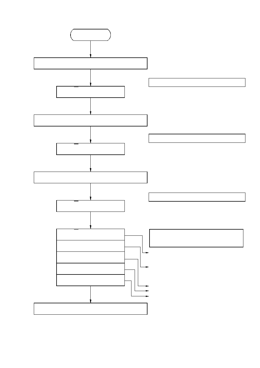
13.Initializing of LCM
Power on
RS R/W DB7 DB6 DB5 DB4 DB3 DB2 DB1 DB0
0
0
0
0
1
1
*
*
*
*
Wait for more than 15 ms after V
CC
rises to 4.5 V
Wait for more than 4.1 ms
1
DB4
DB7
0
RS
0
R/W
DB6
0
0
DB5
1
DB1
DB2
DB3
*
*
*
*
DB0
Wait for more than 100
�s
DB4
1
DB7
R/W
RS
0
0
DB5
DB6
0
0
1
DB1
DB3 DB2
*
*
*
DB0
*
1
DB4
DB7
0
0
RS R/W
1
0
0
DB6 DB5
DB1
F
*
N
DB2
DB3
*
DB0
0
0
0
0
0
0
1
0
0
0
0
0
0
0
0
0
0
0
0
1
0
0
0
0
0
0
0
1
I/D
S
Initialization ends
BF can not be checked before this instruction.
Function set ( Interface is 8 bits long. )
Function set ( Interface is 8 bits long. )
BF can not be checked before this instruction.
BF can not be checked before this instruction.
Function set ( Interface is 8 bits long. )
BF can be checked after the following instructions.
When BF is not checked , the waiting time between
instructions is longer than execution instruction time.
Function set ( Interface is 8 bits long. Specify
the number of display lines and font. )
The number of display lines and character font
can not be changed after this point.
8-Bit Ineterface
Display off
Display clear
Entry mode set
www.dblectro.com
17 19
Power on
RS R/W DB7 DB6 DB5 DB4
0
0
0
0
1
1
Wait for more than 15 ms after V
CC
rises to 4.5 V
Wait for more than 4.1 ms
Wait for more than 100
�s
0
DB4
DB7
0
0
RS R/W
1
0
0
DB6 DB5
0
0
0
0
1
0
0
0
N
F
*
*
0
0
0
0
0
0
Initialization ends
BF can not be checked before this instruction.
Function set ( Interface is 8 bits long. )
Function set ( Interface is 8 bits long. )
BF can not be checked before this instruction.
BF can not be checked before this instruction.
Function set ( Interface is 8 bits long. )
BF can be checked after the following instructions.
When BF is not checked , the waiting time between
instructions is longer than execution instruction time.
Function set ( Set interface to be 4 bits long. )
Interface is 8 bits in length.
Function set ( Interface is 4 bits long. Specify
the number of display lines and character font. )
The number of display lines and character font
can not be changed after this point.
Display off
Display clear
Entry mode set
4-Bit Ineterface
0
DB6
RS R/W
0
0
DB7
0
DB4
DB5
1
1
DB6
0
RS R/W
0
0
DB7
0
DB4
DB5
1
1
0
0
1
0
0
0
0
0
0
0
0
0
0
0
0
0
0
1
0
0
0
0
0
0
0
0
0
I/D
S
1
www.dblectro.com

18 19
14.Quality Assurance
Screen Cosmetic Criteria
Item Defect
Judgment
Criterion
Partition
1 Spots
A)Clear
Size: d mm Acceptable Qty in active area
d
0.1 Disregard
0.1<d
0.2 6
0.2<d
0.3 2
0.3<d 0
Note: Including pin holes and defective dots which must
be within one pixel size.
B)Unclear
Size: d mm Acceptable Qty in active area
d
0.2 Disregard
0.2<d
0.5 6
0.5<d
0.7 2
0.7<d 0
Minor
2
Bubbles in Polarize
Size: d mm Acceptable Qty in active area
d
0.3 Disregard
0.3<d
1.0 3
1.0<d
1.5 1
1.5<d 0
Minor
3 Scratch
In accordance with spots cosmetic criteria. When the light
reflects on the panel surface, the scratches are not to be
remarkable.
Minor
4 Allowable
Density
Above defects should be separated more than 30mm each
other.
Minor
5 Coloration
Not to be noticeable coloration in the viewing area of the
LCD panels.
Back-light type should be judged with back-light on state
only.
Minor
www.dblectro.com

19 19
15.Reliability
Content of Reliability Test
Environmental Test
Test Item
Content of Test
Test Condition
Applicable
Standard
High
Temperature
storage
Endurance test applying the high storage
temperature for a long time.
70
200hrs
----
Low
Temperature
storage
Endurance test applying the high storage
temperature for a long time.
-30
200hrs
----
High
Temperature
Operation
Endurance test applying the electric stress
(Voltage & Current) and the thermal stress
to the element for a long time.
50
200hrs
----
Low
Temperature
Operation
Endurance test applying the electric stress
under low temperature for a long time.
-20
200hrs
----
High
Temperature/
Humidity
Storage
Endurance test applying the high
temperature and high humidity storage for a
long time.
70
,90%RH
96hrs
----
High
Temperature/
Humidity
Operation
Endurance test applying the electric stress
(Voltage & Current) and temperature /
humidity stress to the element for a long
time.
50
,90%RH
96hrs
----
Temperature
Cycle
Endurance test applying the low and high
temperature cycle.
-20
25 50
30min 5min 30min
1 cycle
-20
/50
10 cycles
----
Mechanical Test
Vibration test
Endurance test applying the vibration
during transportation and using.
10~22Hz
1.5mmp-p
22~500Hz
1.5G
Total 0.5hrs
----
Shock test
Constructional and mechanical endurance
test applying the shock during
transportation.
50G Half sign
wave 11 msedc
3 times of each
direction
----
Atmospheric
pressure test
Endurance test applying the atmospheric
pressure during transportation by air.
115mbar
40hrs
----
Others
Static electricity
test
Endurance test applying the electric stress to
the terminal.
VS=800V,RS=1.5k
CS=100pF
1 time
----
***Supply voltage for logic system=5V. Supply voltage for LCD system =Operating voltage at 25
www.dblectro.com