
Preliminary
DFBM-CF121
Data Sheet
April 27, 2005
Proprietary Information and Specifications are Subject to Change
DFBM-CF121
Bluetooth Module Class 2
Wireless communication
module compliant with
Bluetooth Specification V1.1/ 1.2
FEATURES:
Build-in codec suitable for GPS, Mono_Headset, PCs, Digital
Cameras, Printers ......., etc.
Small size and Low Profile using high-density packaging
technology.
High sensitivity for better reception.
Variable profiles with 4M flash ROM.
Various interfaces: UART, USB and PCM.
Wide operating temperature range: -40~+85
.
Device diagram
TM
TM
BC2 -Flash
FLASH
CODEC
Filter
Balun
UART
USB
SPI/ PIO
Speaker / M IC
Or PCM
X'TAL
ANT
BC2 -
CODEC
Filter
Balun
UART
USB
SPI/ PIO
Speaker / M IC
Or PCM
X'TAL
ANT

Preliminary
DFBM-CF121
Data Sheet
April 27, 2005
Proprietary Information and Specifications are Subject to Change
Interface
Interface Description
Antenna
External Antenna 50
UART Interface
TX, RX, RTS, CTS(9600bps~1.5Mbps)
SPI Interface
Synchronous Serial Interface for firmware
download
USB Interface
Full speed Universal Serial Bus interface
PCM Codec
Qualcomm MSM 3000/5000 ,
Motorola MC145483/ MC145481
OKI MSM7705 , STW 5093/5094
PIO Interface
8 terminals
AIO Interface
2 terminals
Rating
Min
Max
Unit
Storage Temperature
-40 +85
VDD_1.8V
-0.4 +1.9
V
VDD_3.15V
-0.4 +3.6
V
Recommend
Min
Max
Unit
VDD_1.8V
+1.7 +1.9
V
VDD_3.15V
+2.7 +3.6
V
Preliminary
DFBM-CF121
Data Sheet
April 27, 2005
Proprietary Information and Specifications are Subject to Change
Current consumption
Typical Average Current Consumption
VDD=1.8V Temperature = +20
∞C Output Power = +3dBm
Mode Avg
Unit
SCO connection HV3 (30ms interval Sniff Mode) (Slave)
26.0
mA
SCO connection HV3 (30ms interval Sniff Mode) (Master)
26.0
mA
SCO connection HV3 (No Sniff Mode) (Slave)
32.0
mA
SCO connection HV1 (Slave)
43.0
mA
SCO connection HV1 (Master)
43.0
mA
ACL data transfer 115.2kbps UART no traffic (Master)
7.0
mA
ACL data transfer 115.2kbps UART no traffic (Slave)
24.0
mA
ACL data transfer 720kbps UART (Master or Slave)
50.0
mA
ACL data transfer 720kbps USB (Master or Slave)
50.0
mA
ACL connection, Sniff Mode 40ms interval, 38.4kbps UART
4.0
mA
ACL connection, Sniff Mode 1.28s interval, 38.4kbps UART
0.5
mA
Parked Slave, 1.28s beacon interval, 38.4kbps UART
0.6
mA
Standby Mode (Connected to host, no RF activity)
85.0
µA
Reset (RST high or RSTB low)
55.0
µA
Preliminary
DFBM-CF121
Data Sheet
April 27, 2005
Proprietary Information and Specifications are Subject to Change
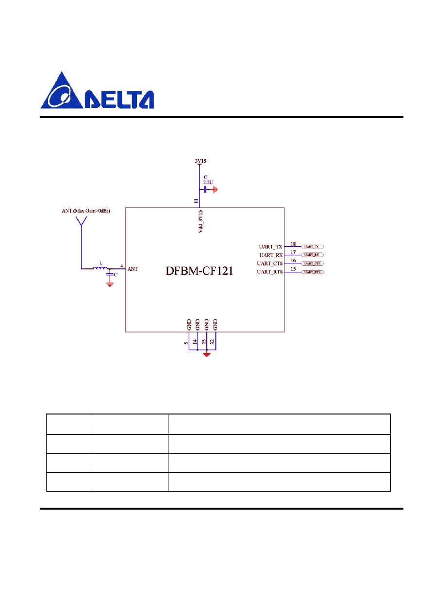
Application circuit
Pin description
Pin No.
Name
Description
1
Reset
An active high reset
2
AIO_1
Analogue Programmable input/output
3
AIO_0
Analogue Programmable input/output
