
Preliminary
DLBM-CH122
Data Sheet
May 19, 2005
Proprietary Information and Specifications are Subject to Change
DLBM-CH122
Bluetooth Module Class 2
A Class 2 Bluetooth module suitable
for cellular phone, smart phone
applications.
1.FEATURES:
Support DUN, SPP, AG & FAX profiles.
Minimal software effort to own Bluetooth functions.
Almost no resource required from host CPU.
Reducing the size and thickness greatly by using high-density
packaging technology.
Compliant to various interfaces: UART, USB, PIO ....
Wide operating temperature range: -30~+80
.
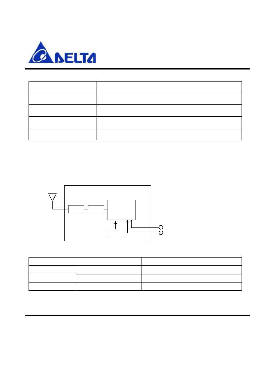
2.Device diagram
BC2 -Flash
FLASH
CODEC
Filter
Balun
UART
USB
SPI/ PIO
Speaker / MIC
Or PCM
X'TAL
ANT
BC2 -
CODEC
Filter
Balun
UART
USB
SPI/ PIO
Speaker / MIC
Or PCM
X'TAL
ANT
Figure 1. DLBM-CH122 Block Diagram
TM
TM
handphone
Preliminary
DLBM-CH122
Data Sheet
May 19, 2005
Proprietary Information and Specifications are Subject to Change
3.General Specification
Bluetooth Specification
Version 1.1
Frequency
2402~2480MHz
Modulation
FHSS/GFSK
Transmission rate
721kbps
Receive sensitivity
-80 dBm
Maximum output power
+4dBm(Class 2)
Operating Voltage
2.7~3.6V
Operating temperature
-30~+80
Antenna Impedance
50 ohm
Package size
9.1*7.9*1.6mm
Operating range
< 10 meters
Current consumption (TX)
< 35mA
Current consumption (Standby)
< 2mA
4.Rating
Min
Max
Unit
Storage Temperature
-40 +85
VDD_1.8V
-0.4 +1.9
V
VDD_IO
-0.4 +3.6
V
VREG_IN
-0.4 +3.6
V
TM
Preliminary
DLBM-CH122
Data Sheet
May 19, 2005
Proprietary Information and Specifications are Subject to Change
5.Interface
Interface Description
Antenna
External Antenna 50 ohm
UART Interface
TX,RX,RTS,CTS(9600bps~1.5Mbps)
SPI Interface
Synchronous Serial Interface for firmware download
PIO Interface
9 terminals
6.Power Supply Diagram
Figure 2. Power Supply Diagram
Terminal
VDD=3.0V
VDD=1.8V
VDD_1.8V
NC 1.7
to
1.9V
VDD_IO
2.7 to 3.6V
1.7 to 3.6V
VREG_IN
2.7 to 3.6V
NC
ANT
X'tal
BPF
BC2-handphone
VDD_IO
VREG_IN
Balun

Preliminary
DLBM-CH122
Data Sheet
May 19, 2005
Proprietary Information and Specifications are Subject to Change
7.RF Characteristics
Operating Condition: +25
, VDD=2.7V
RF Characteristics
Min.
Typ.
Max.
Unit
1. Frequency Range
2400 ~ 2483.5
MHz
2. Output Power
0
4
dBm
3. Sensitivity at 0.1% BER
1) 2402MHz
-82
dBm
2) 2441MHz
-82
dBm
3) 2480MHz
-82
dBm
4. Maximum Input Level (BER
0.1%)
3
dBm
5. Adjacent channel selectivity
1) C/I F=F
0
+ 1MHz
-4
0
dB
2) C/I F=F
0
- 1MHz
-4
0
dB
3) C/I F=F
0
+ 2MHz
-35
-30
dB
4) C/I F=F
0
- 2MHz
-21
-20
dB
5) C/I F
F
0
+ 3MHz
-45
dB
6) C/I F
F
0
- 5MHz
-45
dB
7) C/I F=F
Image
-18
-9
dB
6. Adjacent channel transmit power
1) F=F
0
�
2MHz
-35
dBc
2) F=F
0
�
3MHz
-55
dBc
7. Modulation Characteristics
1) Modulation
f1avg
165
kHz
2) Modulation
f2max
155
-
kHz
8. Initial Carrier Frequency Tolerance
1) 2402MHz
-75
-3
75
kHz
2) 2441MHz
-75
-7
75
kHz
3) 2480MHz
-75
-14
75
kHz

Preliminary
DLBM-CH122
Data Sheet
May 19, 2005
Proprietary Information and Specifications are Subject to Change
9. Carrier Frequency Drift
1) 1slot
9
kHz
2) 5slot
10
kHz
4) Drift rate
8
KHz/50us
10. 20dB Bandwidth for modulated carrier
1) 2402MHz
879
KHz
2) 2441MHz
816
KHz
3) 2480MHz
819
KHz
11.C/I co - channel
9
dB
Preliminary
DLBM-CH122
Data Sheet
May 19, 2005
Proprietary Information and Specifications are Subject to Change
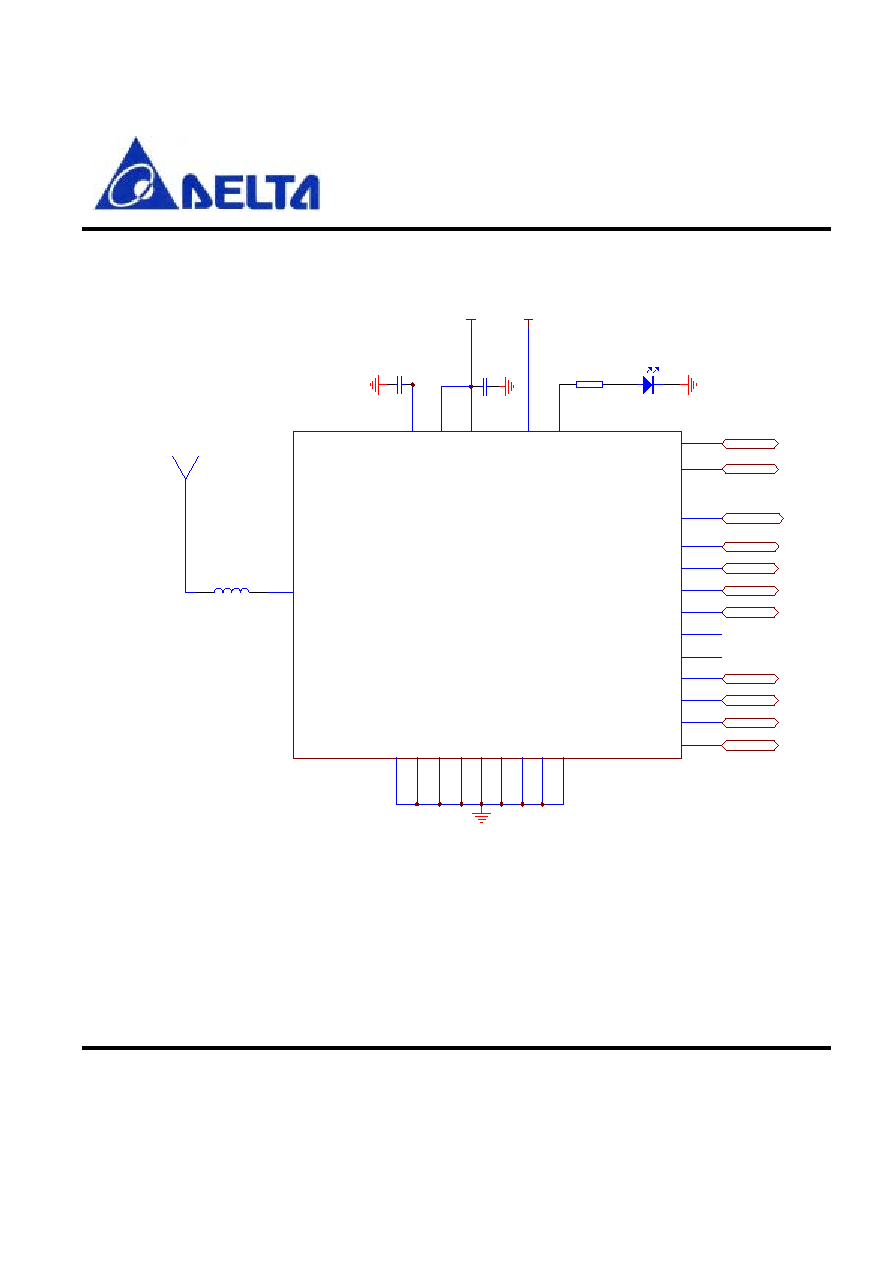
8.Application circuit
***Important: The circuit is offered without warranty and Delta is unable to accept any liability for
direct or consequential loss associated with their use. It is therefore important for designers to
ensure that their Bluetooth handphone design is properly evaluated in a Design Verification
Test. The results of the Design Verification Test should be used to assess the suitability of the
handphone for manufacture.***
Figure 3. 2.7~3.6V Supply
ANT
MIC_N
MIC_P
SPKR_N
SPKR_P
GND
UART_TX
UART_RX
UART_RTS
UART_CTS
VDD_1.8V
VDD_IO
VREG_IN
DLBM-CH121
GND
GND
GND
GND
GND
GND
GND
13
14
29
30
31
12
7
8
GND
9
17
16
15
21
22
20
3
4
23
5
6
10
UART_TX
UART_RX
SPKR_P
SPKR_N
MIC_P
MIC_N
C
2.2U
ANT (Max Gain>0dBi)
3V15
PIO_0
RESET B
24
34
AUDIO_SEL
RESET B
PIO_11
PIO_2
33
1
R
100ohm
D
LED
3V15
32
PIO_1
DISCONNECT
L
1.8nH
25
PIO_4
PIO_5
DATA_SEL
PWR_UP
26
C
2.2U
DLBM-CH122
Preliminary
DLBM-CH122
Data Sheet
May 19, 2005
Proprietary Information and Specifications are Subject to Change
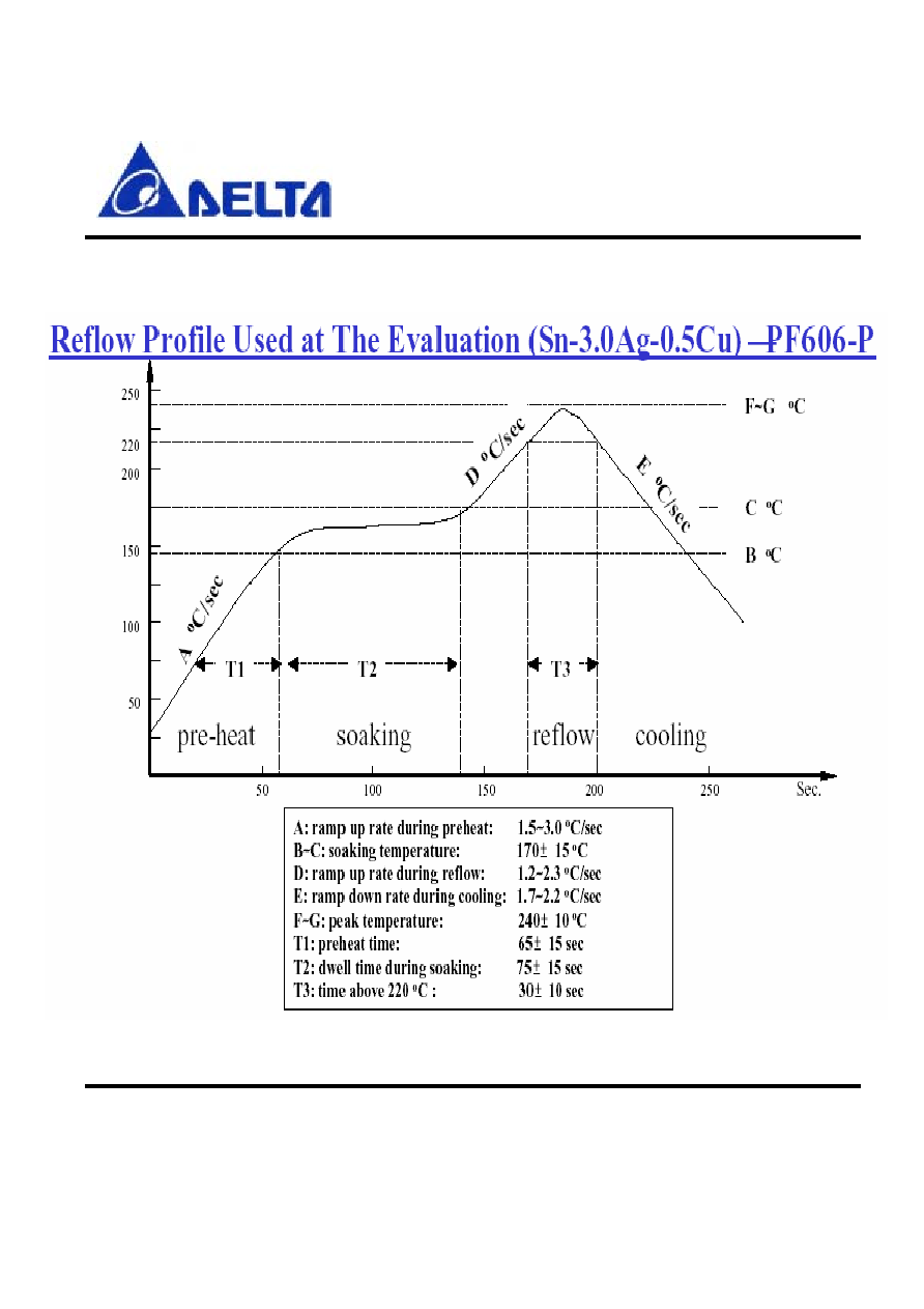
9. RECOMMENDED REFLOW PROFILE
Figure 4. REFLOW PROFILE
Preliminary
DLBM-CH122
Data Sheet
May 19, 2005
Proprietary Information and Specifications are Subject to Change
10.Pin description
Pin No.
Name
Description
1
PIO_11
Programmable I/O terminal
2
PIO_9
Programmable I/O terminal
3
SPKR_P
Speaker output positive
4
SPKR_N
Speaker output negative
5
MIC_P Microphone
input
positive
6
MIC_N Microphone
input
negative
7
Gnd
8
Gnd
9
Gnd
10
ANT RF
input/output
11
AIO_0 Programmable
input/output
12
Gnd
13
Gnd
14
Gnd
15
Vdd_1.8V
Refer to Power supply diagram
16
VREG_IN
Refer to Power supply diagram

Preliminary
DLBM-CH122
Data Sheet
May 19, 2005
Proprietary Information and Specifications are Subject to Change
17
VDD_IO
Refer to Power supply diagram
18
USB_DN USB
data
minus
19
USB_DP
USB data plus with selectable internal
1.5kohm pull-up resistor
20
UART_TX
UART data output active high
21
UART_RX
UART data input active high
22
UART_CTS
UART clear to send active low
23
UART_RTS
UART request to send active low
24
Reset_B Reset
if
low
25
PIO_4
Programmable input/output line
26
PIO_5
Programmable input/output line
27
PIO_10
Programmable input/output line
28
PIO_3
Programmable input/output line
29
Gnd
30
Gnd
31
Gnd
32
PIO_2
Programmable input/output line
33
PIO_1
Programmable input/output line
34
PIO_0
Programmable input/output line
35
SPI_MOSI
Serial Peripheral Interface data input
36
SPI_MISO
Serial Peripheral Interface data output

Preliminary
DLBM-CH122
Data Sheet
May 19, 2005
Proprietary Information and Specifications are Subject to Change
37
SPI_CLK
Serial Peripheral Interface clock
38
SPI_CSB
Chip select for Serial Peripheral Interface,
active low

Preliminary
DLBM-CH122
Data Sheet
May 19, 2005
Proprietary Information and Specifications are Subject to Change
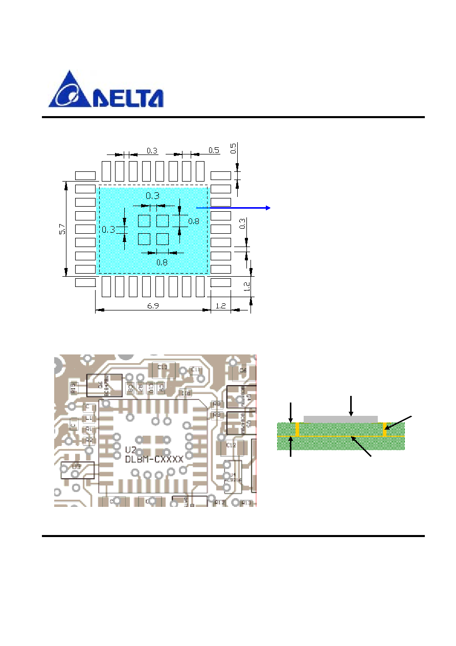
11.Dimensions (mm)
Figure 5. Output pin dimensions
Preliminary
DLBM-CH122
Data Sheet
May 19, 2005
Proprietary Information and Specifications are Subject to Change
12. Layout Guide
Unit: mm
Don't place the ground on the top
layer (Inside area)
Figure 6. Land Pattern
Figure 7. Layout Example
Side View
DLBM-C**2*
Ground VIA
Main Ground plant
T5mil
Preliminary
DLBM-CH122
Data Sheet
May 19, 2005
Proprietary Information and Specifications are Subject to Change
13. Record of changes
Date
Content of change
Maker
May 19,2005
Initial release
JOHNNIE
Contact information
:
Website:
http://www.deltaww.com
Email:
RICHARD.MENG@delta.com.tw
Tel No.: 886-3-3591968#2930