DVFL2800D Series
1X011DSG
11314 4th Avenue
West, Suite 206
Everett, WA 98204
http://www.vpt-inc.com
Sales Information:
Phone: (425) 353-3010
Fax: (425) 353-4030
E-mail: vptsales@vpt-inc.com
1
HIGH RELIABILITY HYBRID
DC-DC CONVERTERS
DESCRIPTION
The DVFL series of high reliability DC-DC converters
is operable over the full military (-55 ∞C to +125 ∞C)
temperature range with no power derating. Unique
to the DVFL series is a magnetic feedback circuit
that is radiation immune. Operating at a nominal
fixed frequency of 500 kHz, these regulated, isolated
units utilize well-controlled undervoltage lockout
circuitry to eliminate slow start-up problems. The
current sharing function allows a maximum of five
units to be connected in parallel to boost the total
output power to 5 times. The output voltage is
trimmable up to +10% or down ≠20%.
These converters are designed and manufactured in
a facility qualified to ISO9001 and certified to MIL-
PRF-38534 and MIL-STD-883.
This product may incorporate one or more of the
following U.S. patents:
5,784,266
5,790,389
5,963,438
5,999,433
6,005,780
6,084,792
6,118,673
FEATURES
∑ High
Reliability
∑ Parallel Up to 5 Units With Current Sharing
∑ Output Voltage Trim Up +10% or Down ≠20%
∑ Wide Input Voltage Range: 16 to 40 Volts per
MIL-STD-704
∑ Up to 120 Watts Output Power
∑ Radiation Immune Magnetic Feedback Circuit
∑ NO Use of Optoisolators
∑ Undervoltage
Lockout
∑ Indefinite Short Circuit Protection
∑ Current Limit Protection
∑ Industry Standard Pinout
∑ Input Transient Voltage: 50 Volts for 1 second
∑ Radiation Hardened Version Available
∑ Precision Seam Welded Hermetic Package
∑ High Power Density: > 80 W/in
3
∑ Custom Versions Available
∑ Additional Environmental Screening Available
∑ Meets MIL-STD-461C and MIL-STD-461D EMC
Requirements When Used With a DVME28 EMI
Filter
∑ MIL-PRF-38534 Element Evaluated
Components
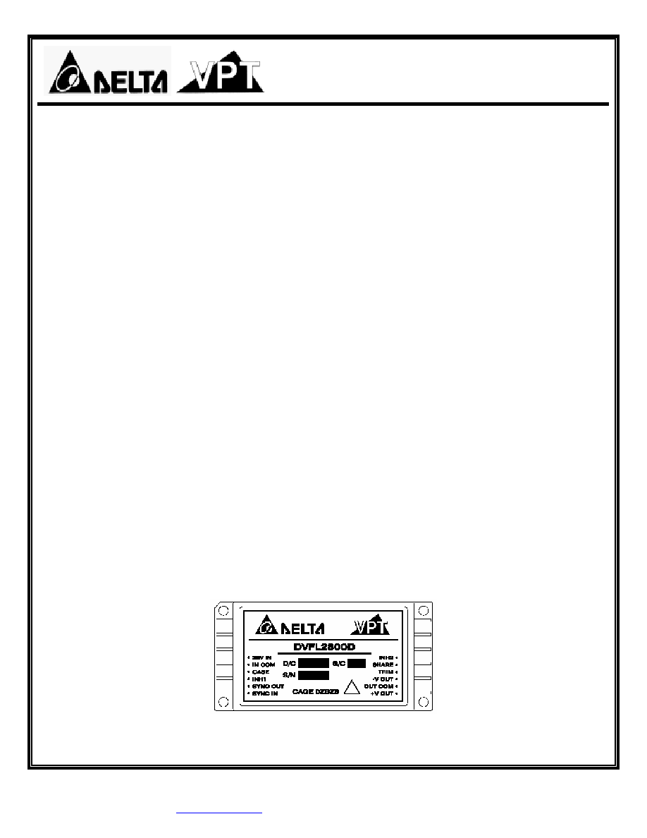
Figure 1 ≠ DVFL2800D DC-DC Converter
(Not To Scale)
DVFL2800D Series
1X011DSG
2
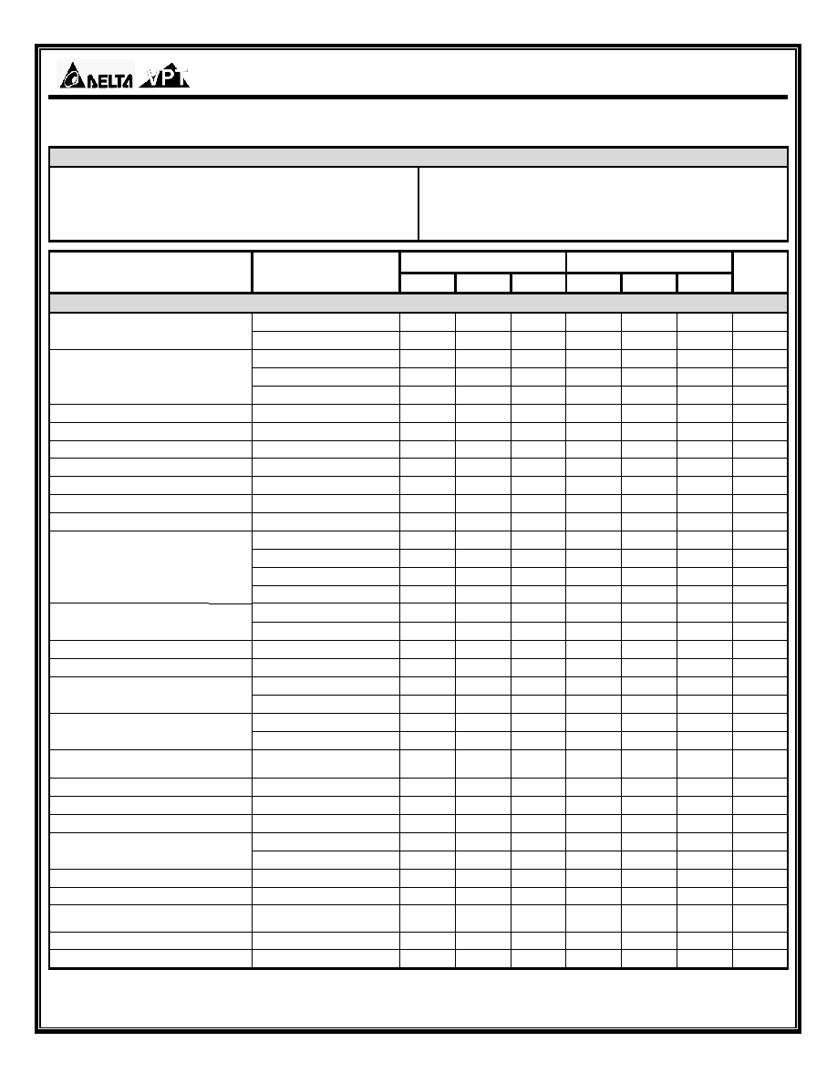
SPECIFICATIONS
(T
CASE
= -55∞C to +125∞C, V
IN
= +28V ± 5%, Full Load
5
, Unless Otherwise Specified)
ABSOLUTE MAXIMUM RATINGS
Input Voltage (Continuous)
40 V
DC
Junction Temperature Rise to Case
+15∞C
Input Voltage (Transient, 1 second)
50 Volts
Storage Temperature
-65∞C to +150∞C
Output Power
1
120 Watts
Lead Solder Temperature (10 seconds)
270∞C
Power Dissipation (Full Load, T
CASE
= +125∞C)
40 Watts
Weight (Maximum) (No Pin Extensions)
86 Grams
DVFL2805D DVFL2812D
Parameter Conditions
Min Typ Max Min Typ Max
Units
STATIC
Continuous
16 28 40 16 28 40 V
INPUT
Voltage
4
Transient,
1
sec
- - 50 - - 50 V
Inhibited
1
- - 3 - - 3
mA
Inhibited
2
- - 70 - - 70
mA
Current
No
Load
- - 140 - - 140
mA
Ripple Current
Full Load
5
,
20Hz
to
10MHz
- - 80 - - 80
mA
p-p
INH1 Pin Input
4
0 - 1.5 0 - 1.5
V
INH2 Pin Input
4
0 - 1.0 0 - 1.0
V
INH1 Pin Open Circuit Voltage
4
10.5 - 13.5
10.5 - 13.5 V
INH2 Pin Open Circuit Voltage
4
5.0 - 8.0 5.0 - 8.0 V
UVLO Turn On
14.0
-
16.0
14.0
-
16.0
V
UVLO Turn Off
4
11.0 - 14.5
11.0 - 14.5 V
+V
OUT
T
CASE
= 25∞C
4.95
5.00
5.05
11.88
12.00
12.12
V
+V
OUT
T
CASE
=
-55∞C
to
+125∞C 4.925 5.00 5.075 11.82 12.00 12.18 V
-V
OUT
T
CASE
= 25∞C
4.80
5.00
5.20
11.80
12.00
12.20
V
OUTPUT
Voltage
5
-V
OUT
T
CASE
= -55∞C to +125∞C
4.75
5.00
5.25
11.52
12.00
12.48
V
Total
- - 100 - - 110 W
Power
3,6
±V
OUT
Either
Output
- - 70 - - 77 W
Current
3,6
±V
OUT
Either
Output
- - 14 - - 6.4 A
Ripple Voltage
±V
OUT
Full Load
5
,
20Hz
to
10MHz
- - 80 - - 80
mV
p-p
+V
OUT
V
IN
= 16V to 40V
-
-
20
-
-
20
mV
Line Regulation
-V
OUT
V
IN
= 16V to 40V
-
-
200
-
-
200
mV
+V
OUT
No Load to Full Load
5
- - 100 - - 120
mV
Load Regulation
-V
OUT
No Load to Full Load
5
- - 200 - - 200
mV
Cross Regulation
-V
OUT
V1+ Load 30% - Load 70%
V2+ Load 70% - Load 30%
- - 450 - - 450
mV
Voltage Trim
Full Load
-20 - 10 -20 - 10 %
Share Pin Voltage
4
2.0 - 3.0 2.0 - 3.0 V
EFFICIENCY Full
Load
5
73 - - 80 - - %
Overload
4
- - 80 - - 80 W
LOAD FAULT POWER DISSIPATION
Short
Circuit
- - 80 - - 80 W
CAPACITIVE LOAD
4
- - 500 - - 500
µF
SWITCHING
FREQUENCY
425 500 600 425 500 600 kHz
SYNC FREQUENCY RANGE
V
H
≠ V
L
= 5V
Duty Cycle = 20% - 80%
500 - 600
500 - 600
kHz
ISOLATION 500
V
DC
, T
CASE
=
25∞C 100 - - 100 - - M
MTBF (MIL-HDBK-217F)
AIF @ T
C
=
55∞C
- 400 - - 400 - kHrs
DVFL2800D Series
1X011DSG
3
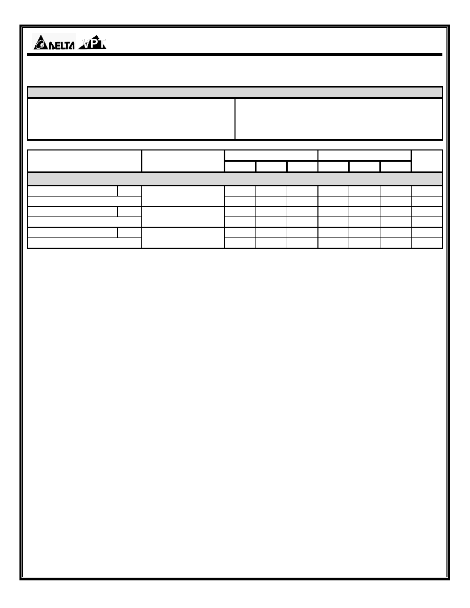
SPECIFICATIONS
(T
CASE
= -55∞C to +125∞C, V
IN
= +28V ± 5%, Full Load
5
, Unless Otherwise Specified)
ABSOLUTE MAXIMUM RATINGS
Input Voltage (Continuous)
40 V
DC
Junction Temperature Rise to Case
+15∞C
Input Voltage (Transient, 1 second)
50 Volts
Storage Temperature
-65∞C to +150∞C
Output Power
1
120 Watts
Lead Solder Temperature (10 seconds)
270∞C
Power Dissipation (Full Load, T
CASE
= +125∞C)
40 Watts
Weight (Maximum) (No Pin Extensions)
86 Grams
DVFL2805D DVFL2812D
Parameter Conditions
Min Typ Max Min Typ Max
Units
DYNAMIC
Load Step Output Transient
±V
OUT
- - 400 - - 500
mV
PK
Load Step Recovery
2
Half Load to Full Load
- - 500 - - 500
µSec
Line Step Output Transient
4
±V
OUT
- 300
600 - 600
1200
mV
PK
Line Step Recovery
2, 4
V
IN
= 16V to 40V
- 300
500 - 300
500
µSec
Turn On Delay
±V
OUT
- - 20 - - 20
mSec
Turn On Overshoot
V
IN
= 0V to 28V
- - 25 - - 50
mV
PK
Notes: 1. Dependant on output voltage.
2. Time for output voltage to settle within 1% of its nominal value.
3. Derate linearly to 0 at 135∞C.
4. Verified by qualification testing.
5. Half load at +V
OUT
and half load at ≠V
OUT
.
6. Up to 70% of the total power or current can be drawn from any one of the two outputs.
DVFL2800D Series
1X011DSG
4
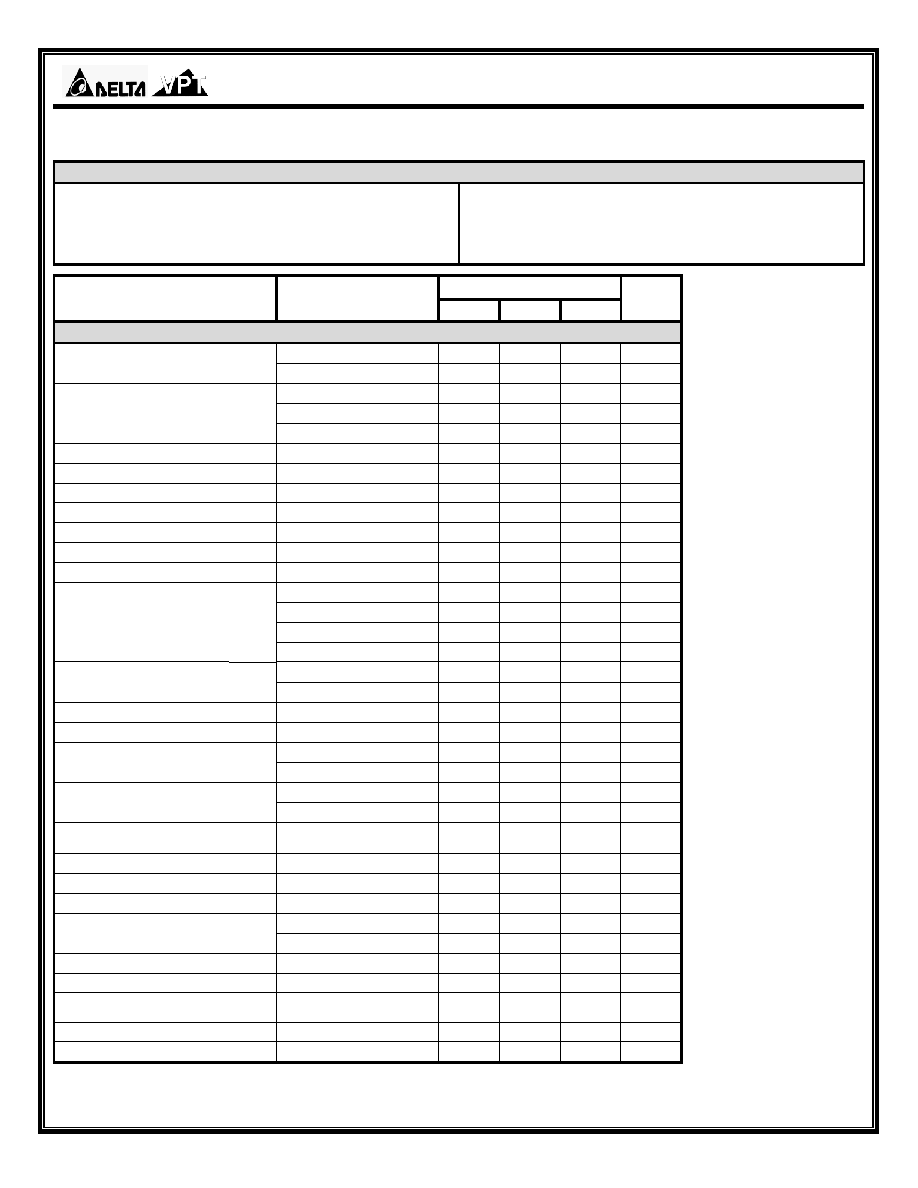
SPECIFICATIONS
(T
CASE
= -55∞C to +125∞C, V
IN
= +28V ± 5%, Full Load
5
, Unless Otherwise Specified)
ABSOLUTE MAXIMUM RATINGS
Input Voltage (Continuous)
40 V
DC
Junction Temperature Rise to Case
+15∞C
Input Voltage (Transient, 1 second)
50 Volts
Storage Temperature
-65∞C to +150∞C
Output Power
1
120 Watts
Lead Solder Temperature (10 seconds)
270∞C
Power Dissipation (Full Load, T
CASE
= +125∞C)
40 Watts
Weight (Maximum) (No Pin Extensions)
86 Grams
DVFL2815D
Parameter Conditions
Min Typ Max
Units
STATIC
Continuous
16 28 40 V
INPUT
Voltage
4
Transient, 1 sec
-
-
50
V
Inhibited 1
-
-
3
mA
Inhibited 2
-
-
70
mA
Current
No Load
-
-
140
mA
Ripple Current
Full Load
5
, 20Hz to 10MHz
-
-
80
mA
p-p
INH1 Pin Input
4
0
-
1.5
V
INH2 Pin Input
4
0
-
1.0
V
INH1 Pin Open Circuit Voltage
4
10.5
-
13.5
V
INH2 Pin Open Circuit Voltage
4
5.0
-
8.0
V
UVLO Turn On
14.5
-
16.0
V
UVLO Turn Off
4
11.0
-
14.5
V
+V
OUT
T
CASE
= 25∞C
14.85
15.00
15.15
V
+V
OUT
T
CASE
= -55∞C to +125∞C
14.775
15.00
15.225
V
-V
OUT
T
CASE
= 25∞C
14.80
15.00
15.20
V
OUTPUT
Voltage
5
-V
OUT
T
CASE
= -55∞C to +125∞C
14.40
15.00
15.60
V
Total
-
-
120
W
Power
3,6
±V
OUT
Either Output
-
-
84
W
Current
3,6
±V
OUT
Either Output
-
-
5.6
A
Ripple Voltage
±V
OUT
Full Load
5
, 20Hz to 10MHz
-
-
80
mV
p-p
+V
OUT
V
IN
= 16V to 40V
-
-
20
mV
Line Regulation
-V
OUT
V
IN
= 16V to 40V
-
-
200
mV
+V
OUT
No Load to Full Load
5
- -
120
mV
Load Regulation
-V
OUT
No Load to Full Load
5
- -
200
mV
Cross Regulation
-V
OUT
V1+ Load 30% - Load 70%
V2+ Load 70% - Load 30%
- -
450
mV
Voltage Trim
Full Load
-20 - 10 %
Share Pin Voltage
4
2.0
-
3.0
V
EFFICIENCY Full
Load
5
81 - - %
Overload
4
- - 80
W
LOAD FAULT POWER DISSIPATION
Short Circuit
-
-
80
W
CAPACITIVE LOAD
4
-
-
500
µF
SWITCHING
FREQUENCY
425 500 600 kHz
SYNC FREQUENCY RANGE
V
H
≠ V
L
= 5V
Duty Cycle = 20% - 80%
500 - 600
kHz
ISOLATION 500
V
DC
, T
CASE
= 25∞C
100
-
-
M
MTBF (MIL-HDBK-217F)
AIF @ T
C
= 55∞C
-
400
-
kHrs
DVFL2800D Series
1X011DSG
5
SPECIFICATIONS
(T
CASE
= -55∞C to +125∞C, V
IN
= +28V ± 5%, Full Load
5
, Unless Otherwise Specified)
ABSOLUTE MAXIMUM RATINGS
Input Voltage (Continuous)
40 V
DC
Junction Temperature Rise to Case
+15∞C
Input Voltage (Transient, 1 second)
50 Volts
Storage Temperature
-65∞C to +150∞C
Output Power
1
120 Watts
Lead Solder Temperature (10 seconds)
270∞C
Power Dissipation (Full Load, T
CASE
= +125∞C)
40 Watts
Weight (Maximum) (No Pin Extensions)
86 Grams
DVFL2815D
Parameter Conditions
Min Typ Max
Units
DYNAMIC
Load Step Output Transient
±V
OUT
- -
500
mV
PK
Load Step Recovery
2
Half Load to Full Load
- -
500
µSec
Line Step Output Transient
4
±V
OUT
- 600
1200
mV
PK
Line Step Recovery
2, 4
V
IN
= 16V to 40V
- 300
500
µSec
Turn On Delay
±V
OUT
- - 20
mSec
Turn On Overshoot
V
IN
= 0V to 28V
- - 50
mV
PK
Notes: 1. Dependant on output voltage.
2. Time for output voltage to settle within 1% of its nominal value.
3. Derate linearly to 0 at 135∞C.
4. Verified by qualification testing.
5. Half load at +V
OUT
and half load at ≠V
OUT
.
6. Up to 70% of the total power or current can be drawn from any one of the two outputs.