DVSB2800D Series
1X046DSD
11314 4th Avenue
West, Suite 206
Everett, WA 98204
http://www.vpt-inc.com
Sales Information:
Phone: (425) 353-3010
Fax: (425) 353-4030
E-mail: vptsales@vpt-inc.com
1
HIGH RELIABILITY HYBRID
DC-DC CONVERTERS
DESCRIPTION
The DVSB series of high reliability DC-DC converters
is operable over the full military (-55∞C to +125∞C)
temperature range with no power derating. Unique
to the DVSB series is a fault tolerant magnetic
feedback circuit. Operating at a nominal fixed
frequency of 325 kHz per stage, these regulated,
isolated units utilize well-controlled undervoltage
lockout circuitry to eliminate slow start-up problems.
These converters are designed and manufactured in
a facility qualified to ISO9001 and certified to MIL-
PRF-38534 and MIL-STD-883.
This product may incorporate one or more of the
following U.S. patents:
5,784,266
5,790,389
5,963,438
5,999,433
6,005,780
6,084,792
6,118,673
FEATURES
∑ High
Reliability
∑ Very Low Output Noise
∑ Wide Input Voltage Range: 15 to 50 Volts per
MIL-STD-704
∑ Up to 12.5 Watts Output Power
∑ Fault Tolerant Magnetic Feedback Circuit
∑ NO Use of Optoisolators
∑ Undervoltage
Lockout
∑ Indefinite Short Circuit Protection
∑ Current Limit Protection
∑ High Input Transient Voltage: 80 Volts for 1 sec
per MIL-STD-704A
∑ Precision Projection Welded Hermetic Package
∑ High
Power
Density
∑ Custom Versions Available
∑ Additional Environmental Screening Available
∑ Meets MIL-STD-461C and MIL-STD-461D EMC
Requirements When Used With a DVMH28 EMI
Filter
∑ Flanged and Non-flanged Versions Available.
∑ MIL-PRF-38534 Element Evaluated
Components
Figure 1
≠ DVSB2800D / DVSB2800DF DC-DC Converter
(Not To Scale)
DVSB2800D Series
1X046DSD
2
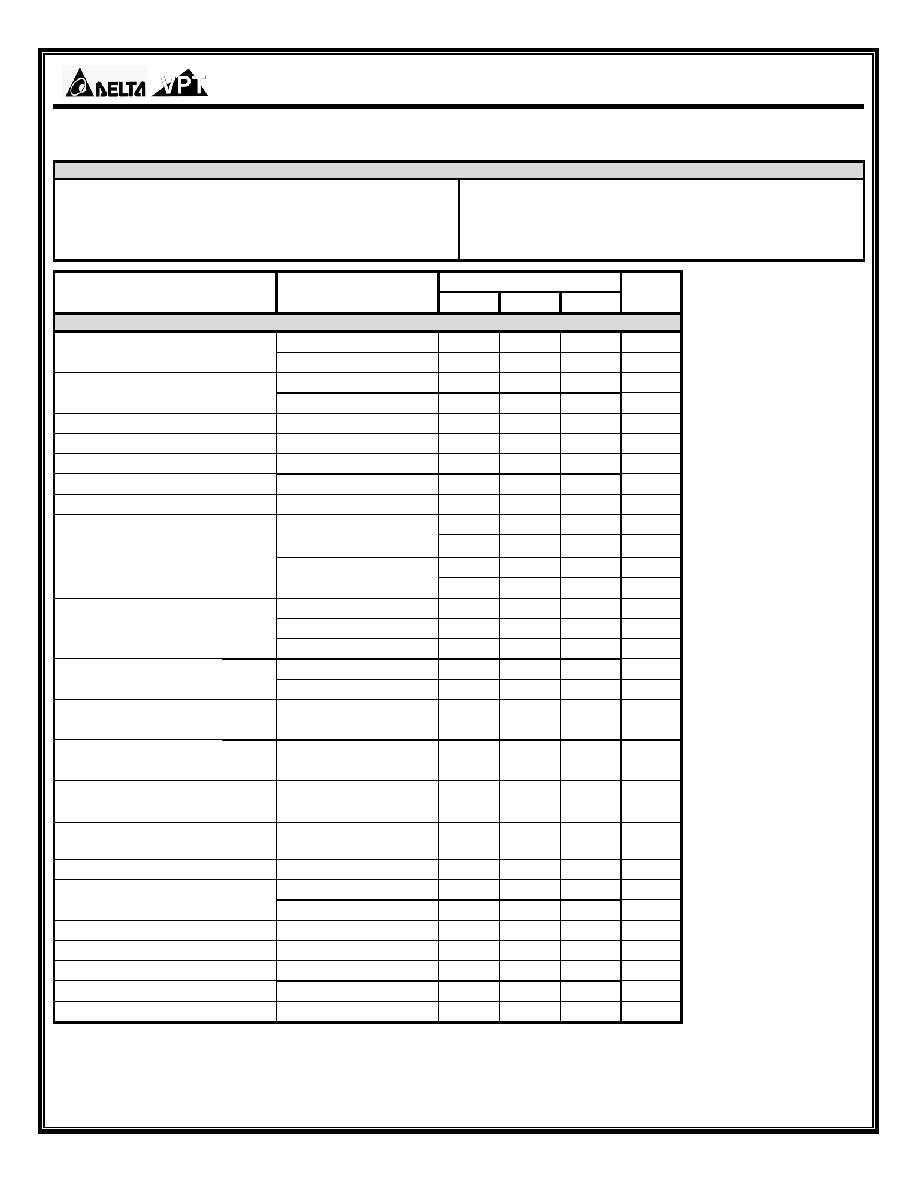
SPECIFICATIONS
(T
CASE
= -55∞C to +125∞C, V
IN
= +28V ± 5%, Full Load, Unless Otherwise Specified)
ABSOLUTE MAXIMUM RATINGS
Input Voltage (Continuous)
50 V
DC
Junction Temperature Rise to Case
+15∞C
Input Voltage (Transient, 1 second)
80 Volts
Storage Temperature
-65∞C to +150∞C
Output Power
12.5 Watts
Lead Solder Temperature (10 seconds)
270∞C
Power Dissipation (Full Load, T
CASE
= +125∞C)
6.0 Watts
Weight (Maximum) (Un-Flanged / Flanged)
(24 / 28) Grams
DVSB2853R3D
Parameter Conditions
Min Typ Max
Units
STATIC
Continuous
15 28 50 V
INPUT
Voltage
4
Transient, 1 sec
4
- - 80 V
Inhibited -
3.5
5.0
mA
Current
No Load
-
-
60
mA
Ripple Current
Full Load, 20Hz to 10MHz
-
40
60
mA
p-p
Inhibit Pin Input
4
0
-
1.5
V
Inhibit Pin Open Circuit Voltage
4
12 14 17 V
UVLO Turn On
10.5
-
14.5
V
UVLO Turn Off
4
9
-
13
V
V
OUT1
4.95 5.0 5.05 V
V
OUT2
T
CASE
= 25∞C
3.267 3.3 3.333 V
V
OUT1
4.925 5.0 5.075 V
OUTPUT
Voltage
V
OUT2
T
CASE
= -55∞C to +125∞C
3.25 3.3 3.35 V
Total
0
-
12.5
W
V
OUT1
0
-
7.5
W
Power
3,4
V
OUT2
0 - 5 W
V
OUT1
0
-
1.5
A
Current
3
V
OUT2
0 - 1.5
A
V
OUT1
Ripple Voltage
V
OUT2
Full Load, 20Hz to 10MHz
-
40
60
mV
p-p
V
OUT1
Line Regulation
V
OUT2
V
IN
= 15V to 50V
-
0
25
mV
V
OUT1
Load Regulation
V
OUT2
No Load to Full Load
- 10 50
mV
V
OUT1
Cross Regulation
V
OUT2
V
OUT1
= 0%, V
OUT2
= 100%
V
OUT1
= 100%, V
OUT2
= 0%
- 10 50
mV
EFFICIENCY Full
Load
69 74 - %
Overload
4
- - 11
W
LOAD FAULT POWER DISSIPATION
Short Circuit
-
-
12
W
CAPACITIVE LOAD
4
Either Output
-
-
500
µF
SWITCHING
FREQUENCY
550 650 700 kHz
SYNCHRONIZATION FREQUENCY
5
700 750 800 kHz
ISOLATION 500
V
DC
, T
CASE
= 25∞C
100
-
-
M
MTBF (MIL-HDBK-217F)
AIF @ T
C
= 55∞C
-
350
-
kHrs
DVSB2800D Series
1X046DSD
3
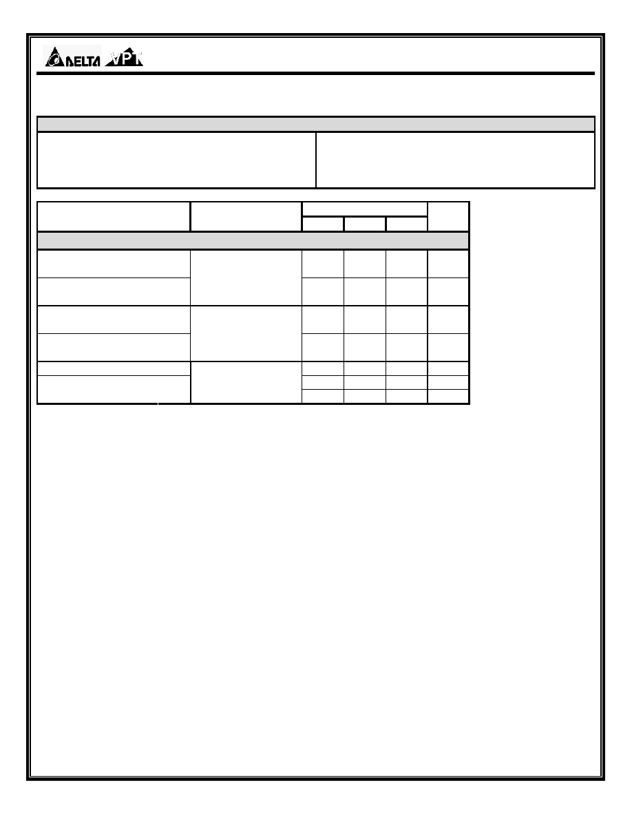
SPECIFICATIONS
(T
CASE
= -55∞C to +125∞C, V
IN
= +28V ± 5%, Full Load, Unless Otherwise Specified)
ABSOLUTE MAXIMUM RATINGS
Input Voltage (Continuous)
50 V
DC
Junction Temperature Rise to Case
+15∞C
Input Voltage (Transient, 1 second)
80 Volts
Storage Temperature
-65∞C to +150∞C
Output Power
12.5 Watts
Lead Solder Temperature (10 seconds)
270∞C
Power Dissipation (Full Load, T
CASE
= +125∞C)
6.0 Watts
Weight (Maximum) (Un-Flanged / Flanged)
(24 / 28) Grams
DVSB2853R3D
Parameter Conditions
Min Typ Max
Units
DYNAMIC
V
OUT1
Load Step Output Transient
V
OUT2
- 200
400
mV
PK
V
OUT1
Load Step Recovery
2
V
OUT2
Half Load to Full Load
- 450
700
µSec
V
OUT1
Line Step Output Transient
4
V
OUT2
- 100
400
mV
PK
V
OUT1
Line Step Recovery
2, 4
V
OUT2
V
IN
= 16V to 40V
- 300
600
µSec
Turn On Delay
- - 20
mSec
V
OUT1
- - 25
mV
PK
Turn On Overshoot
V
OUT2
V
IN
= 0V to 28V
- - 15
mV
PK
Notes: 1. This note intentionally not used.
2. Time for output voltage to settle within 1% of its nominal value.
3. Derate linearly to 0 at 135∞C.
4. Verified by qualification testing.
5. Synchronization is TTL signal with V
SYNC MAX
= 6V.
DVSB2800D Series
1X046DSD
5
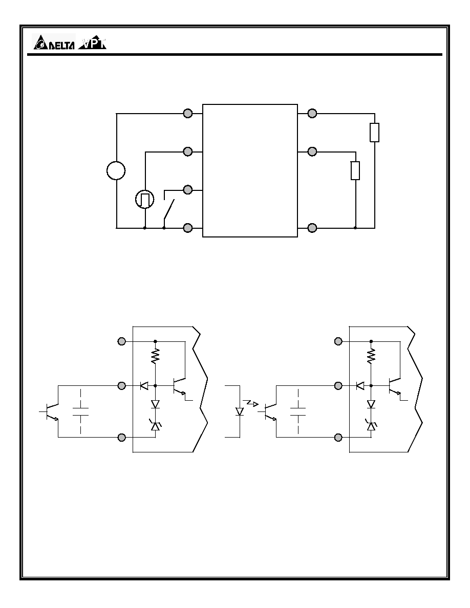
CONNECTION DIAGRAM
8
IN COM
1
INH
9
28V IN
4
+VOUT2
3
OUT COM
LOAD
+
-
28 Vdc
SYNC
7
2
+VOUT1
LOAD
Figure 3
INHIBIT DRIVE CONNECTION DIAGRAMS
8
IN COM
1
INH
9
28V IN
OPTIONAL
CAPACITOR
BIAS
14V
15K
8
IN COM
1
INH
9
28V IN
OPTIONAL
CAPACITOR
BIAS
14V
15K
OPTOISOLATOR
Figure 4
≠ Internal Inhibit Circuit and Recommended Drive
Figure 5
≠ Isolated Inhibit Drive
(Shown with optional capacitor for turn-on delay)
(Shown with optional capacitor for turn-on delay)
