DVTR2800T Series
1X009DSG
11314 4th Avenue
West, Suite 206
Everett, WA 98204
http://www.vpt-inc.com
Sales Information:
Phone: (425) 353-3010
Fax: (425) 353-4030
E-mail: vptsales@vpt-inc.com
1
HIGH RELIABILITY HYBRID
DC-DC CONVERTERS
DESCRIPTION
The DVTR series of high reliability DC-DC converters
is operable over the full military (-55 ∞C to +125 ∞C)
temperature range with no power derating. Unique
to the DVTR series is a fault tolerant magnetic
feedback circuit. Operating at a nominal fixed
frequency of 325 kHz per stage, these regulated,
isolated units utilize well-controlled undervoltage
lockout circuitry to eliminate slow start-up problems.
These converters are designed and manufactured in
a facility qualified to ISO9001 and certified to MIL-
PRF-38534 and MIL-STD-883.
This product may incorporate one or more of the
following U.S. patents:
5,784,266
5,790,389
5,963,438
5,999,433
6,005,780
6,084,792
6,118,673
FEATURES
∑ High
Reliability
∑ Very Low Output Noise
∑ Wide Input Voltage Range: 15 to 50 Volts per
MIL-STD-704
∑ Up to 30 Watts Output Power
∑ Fault Tolerant Magnetic Feedback Circuit
∑ NO Use of Optoisolators
∑ Undervoltage
Lockout
∑ Indefinite Short Circuit Protection
∑ Current Limit Protection
∑ Industry Standard Pinout
∑ High Input Transient Voltage: 80 Volts for 1 sec
per MIL-STD-704A
∑ Precision Seam Welded or Solder Seal
Hermetic Package
∑ High Power Density: > 28 W/in
3
∑ Custom Versions Available
∑ Additional Environmental Screening Available
∑ Meets MIL-STD-461C and MIL-STD-461D EMC
Requirements When Used With a DVMC28 EMI
Filter
∑ Flanged and Non-flanged Versions Available.
∑ MIL-PRF-38534 Element Evaluated
Components
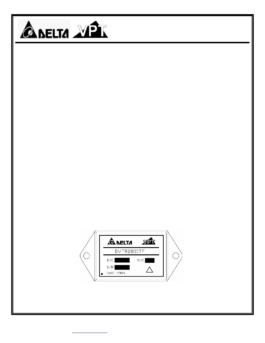
Figure 1
≠ DVTR2800T / DVTR2800TF DC-DC Converter
(Not To Scale)

DVTR2800T Series
1X009DSG
2
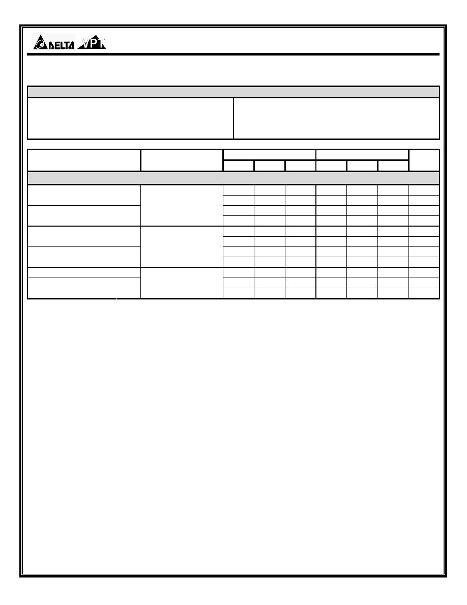
SPECIFICATIONS
(T
CASE
= -55∞C to +125∞C, V
IN
= +28V ± 5%, Full Load
5
, Unless Otherwise Specified)
ABSOLUTE MAXIMUM RATINGS
Input Voltage (Continuous)
50 V
DC
Junction Temperature Rise to Case
+15∞C
Input Voltage (Transient, 1 second)
80 Volts
Storage Temperature
-65∞C to +150∞C
Output Power
30 Watts
Lead Solder Temperature (10 seconds)
270∞C
Power Dissipation (Full Load, T
CASE
= +125∞C)
10 Watts
Weight (Maximum) (Un-Flanged / Flanged)
(50 / 56) Grams
DVTR28512T DVTR28515T
Parameter Conditions
Min Typ Max Min Typ Max
Units
STATIC
Continuous
15 28 50 15 28 50 V
INPUT
Voltage
Transient, 1 sec
4
- - 80 - - 80 V
Inhibited
- 3.5 5 - 3.5 5 mA
Current
No
Load
- 20 50 - 20 50
mA
Ripple Current
Full Load
5
,
20Hz
to
10MHz
- 20 50 - 20 50
mA
p-p
Inhibit Pin Input
4
0 - 1.5 0 - 1.5
V
Inhibit Pin Open Circuit Voltage
4
13 15 17 13 15 17 V
UVLO Turn On
10.5
-
14.5
10.5
-
14.5
V
UVLO Turn Off
4
11.0 - 14.5
11.0 - 14.5 V
V
MAIN
4.95 5.0 5.05 4.95 5.0 5.05 V
+V
AUX
11.88 12.0 12.12 14.85 15.0 15.15 V
-V
AUX
T
CASE
= 25∞C
-12.24 -12.0 -11.76 -15.30 -15.0 -14.70 V
V
MAIN
4.85 5.0 5.15 4.85 5.0 5.15 V
+V
AUX
11.64 12.0 12.36 14.55 15.0 15.45 V
OUTPUT
Voltage
-V
AUX
T
CASE
= -55∞C to +125∞C
-12.48 -12.0 -11.52 -15.60 -15.0 -14.40 V
Total
0
-
30
0
-
30
W
V
MAIN
0 - 15 0 - 15
W
Power
4
±V
AUX
6
0 - 15 0 - 15
W
V
MAIN
0 - 3.0 0 - 3.0
A
Current
3
±V
AUX
Either Output
6
0 -
0.87
0 -
0.70
A
V
MAIN
- 20 60 - 20 60
mV
p-p
Ripple Voltage
±V
AUX
Full Load
5
, 20Hz to 10MHz
- 40
100 - 40
100
mV
p-p
V
MAIN
- 10 25 - 10 25
mV
+V
AUX
- 15 50 - 15 50
mV
Line Regulation
-V
AUX
V
IN
= 15V to 50V
- 20
100 - 20
100
mV
V
MAIN
- 10 25 - 10 25
mV
+V
AUX
- 10 50 - 10 50
mV
Load Regulation
-V
AUX
No Load to Full Load
5,8
- 50
250 - 50
250
mV
Cross Regulation
±V
AUX
+V
OUT
= 30%, -V
OUT
= 70%
+V
OUT
= 70%, -V
OUT
= 30%
- - 550 - - 550
mV
EFFICIENCY Full
Load
5
74 79 - 75 80 - %
Overload
4
- - 15 - - 15 W
LOAD FAULT POWER DISSIPATION
Short
Circuit
- - 10 - - 10 W
CAPACITIVE LOAD
4
- - 500 - - 500
µF
SWITCHING
FREQUENCY
550 650 700 550 650 700 kHz
SYNCHRONIZATION FREQUENCY
7
700 750 800 700 750 800 kHz
ISOLATION 500
V
DC
, T
CASE
=
25∞C 100 - - 100 - - M
MTBF (MIL-HDBK-217F)
AIF @ T
C
=
55∞C
- 307 - - 307 - kHrs
DVTR2800T Series
1X009DSG
3
SPECIFICATIONS
(T
CASE
= -55∞C to +125∞C, V
IN
= +28V ± 5%, Full Load
5
, Unless Otherwise Specified)
ABSOLUTE MAXIMUM RATINGS
Input Voltage (Continuous)
50 V
DC
Junction Temperature Rise to Case
+15∞C
Input Voltage (Transient, 1 second)
80 Volts
Storage Temperature
-65∞C to +150∞C
Output Power
30 Watts
Lead Solder Temperature (10 seconds)
270∞C
Power Dissipation (Full Load, T
CASE
= +125∞C)
10 Watts
Weight (Maximum) (Un-Flanged / Flanged)
(50 / 56) Grams
DVTR28512T DVTR28515T
Parameter Conditions
Min Typ Max Min Typ Max
Units
DYNAMIC
V
MAIN
- 200
400 - 200
400
mV
PK
Load Step Output Transient
±V
AUX
- 500
700 - 500
700
mV
PK
V
MAIN
- 200
400 - 200
400
µSec
Load Step Recovery
2
±V
AUX
Half Load to Full Load
- 200
400 - 200
400
µSec
V
MAIN
- 200
400 - 200
400
mV
PK
Line Step Output Transient
4
±V
AUX
- 300
500 - 300
500
mV
PK
V
MAIN
- 200
400 - 200
400
µSec
Line Step Recovery
2, 4
±V
AUX
V
IN
= 15V to 50V
- 200
400 - 200
400
µSec
Turn On Delay
- - 20 - - 20
mSec
V
MAIN
- - 25 - - 25
mV
PK
Turn On Overshoot
±V
AUX
V
IN
= 0V to 28V
- - 50 - - 50
mV
PK
Notes: 1. This note intentionally not used.
2. Time for output voltage to settle within 1% of its nominal value.
3. Derate linearly to 0 at 135∞C.
4. Verified by qualification testing.
5. 15W on V
MAIN
and 15W on ±V
AUX
.
6. Up to 70% of the total auxiliary power or current can be drawn from either of the auxiliary outputs.
7. Synchronization is TTL signal with V
SYNC MAX
= 6V.
8. -V
AUX
is 5% Load to Full Load at -55∞C.

DVTR2800T Series
1X009DSG
4
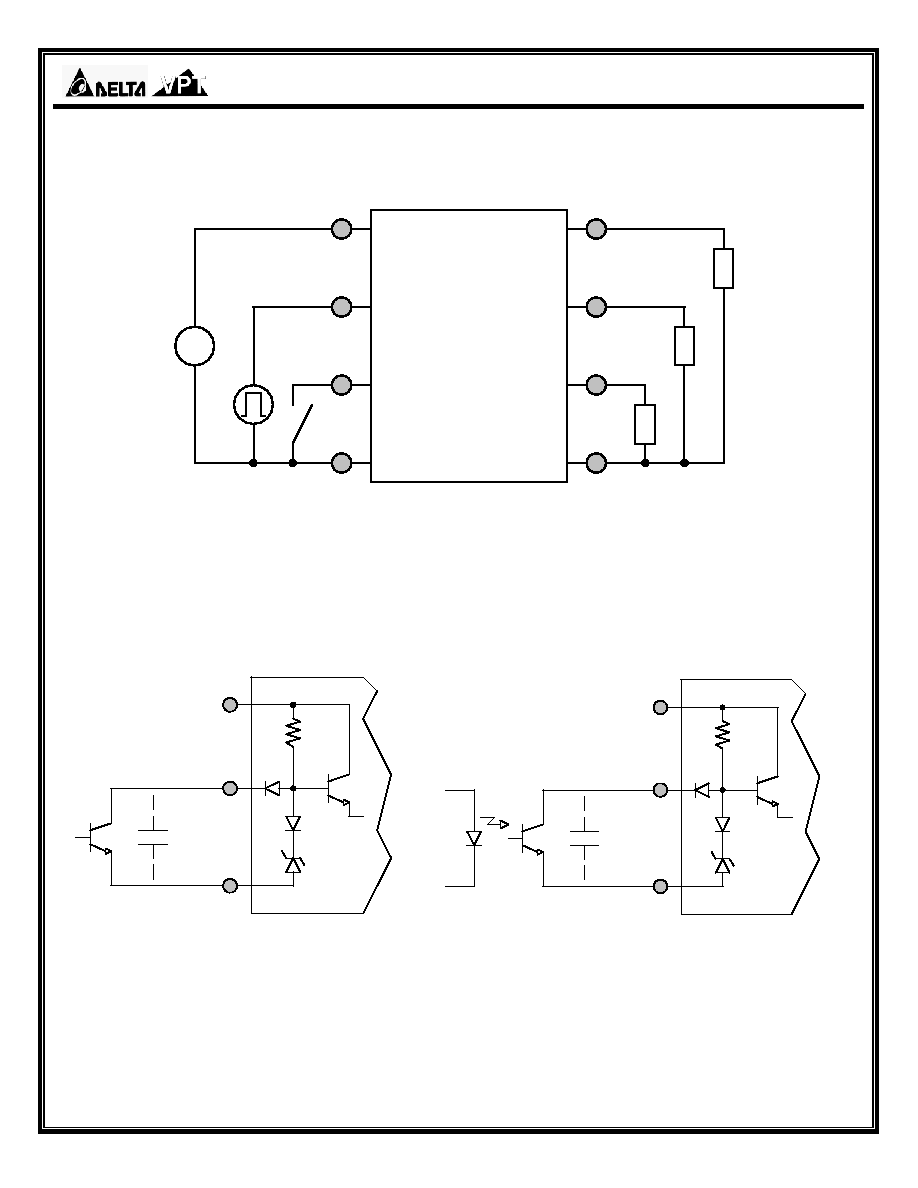
BLOCK DIAGRAM
PRIMARY
HOUSEKEEPING
SUPPLY
DUAL PWM
CONTROLLER
PIN 8
INH
TRANSFORMER
ISOLATED
POWER
FEEDFORWARD
TRANSFORMER
ISOLATED
ERROR SIGNAL
FEEDBACK
VOLTAGE AND
CURRENT ERROR
AMPLIFIERS
SECONDARY
HOUSKEEPING
SUPPLY
IN COM
PIN 10
28V IN
PIN 1
+V MAIN
PIN 2
OUT COM
PIN 3
+V AUX
PIN 5
-V AUX
PIN 4
SYNC
PIN 9
Figure 2
DVTR2800T Series
1X009DSG
5
CONNECTION DIAGRAM
10
IN COM
8
INH
1
28V IN
5
+V AUX
3
OUT COM
LOAD
+
-
28 Vdc
4
-V AUX
LOAD
SYNC
9
2
+V MAIN
LOAD
Figure 3
INHIBIT DRIVE CONNECTION DIAGRAMS
10
IN COM
8
INH
1
28V IN
OPTIONAL
CAPACITOR
BIAS
14V
15K
10
IN COM
8
INH
1
28V IN
OPTIONAL
CAPACITOR
BIAS
14V
15K
OPTOISOLATOR
Figure 4
≠ Internal Inhibit Circuit and Recommended Drive
Figure 5
≠ Isolated Inhibit Drive
(Shown with optional capacitor for turn-on delay)
(Shown with optional capacitor for turn-on delay)
DVTR2800T Series
1X009DSG
6
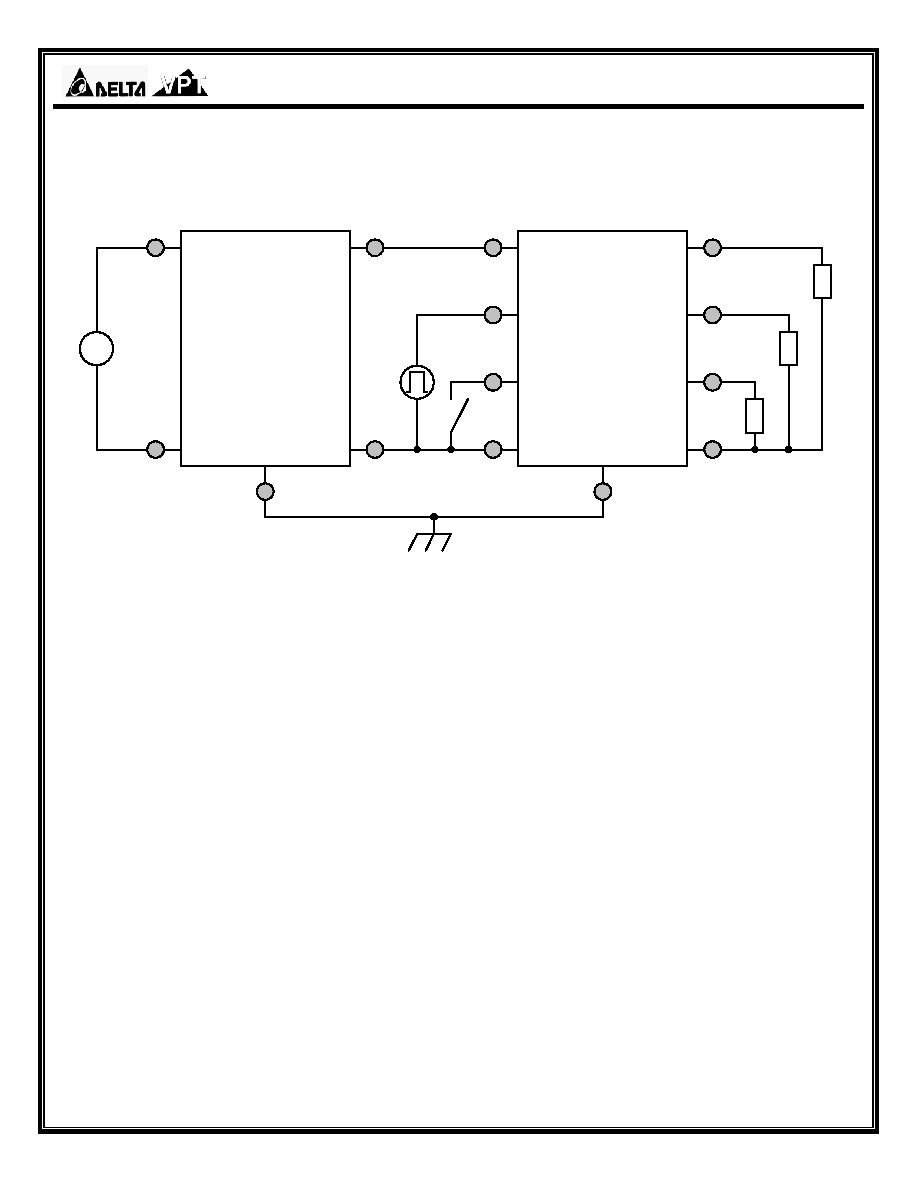
EMI FILTER HOOKUP DIAGRAM
10
IN COM
8
INH
1
28V IN
5
+V AUX
3
OUT COM
LOAD
+
-
28 Vdc
2
28V OUT
4
OUT COM
1
28V IN
5
IN COM
3
DVMC28 EMI FILTER
6, 7
DVTR2800T DC-DC CONVERTER
CASE
4
-V AUX
LOAD
SYNC
9
2
+V MAIN
LOAD
Figure 6
≠ Converter with EMI Filter

DVTR2800T Series
1X009DSG
7
EFFICIENCY PERFORMANCE CURVES
(T
CASE
= 25∞C)
V
IN
= 15V
V
IN
= 28V
V
IN
= 50V
55
60
65
70
75
80
85
-
5
10
15
20
25
30
35
40
Output Power [W]
E
f
f
i
ci
e
n
cy [
%
]
Figure 7
≠ DVTR28512T
Efficiency (%) vs. Output Power (W)
55
60
65
70
75
80
85
-
5
10
15
20
25
30
35
40
Output Power [W]
Effi
ciency [%]
Figure 8
≠ DVTR28515T
Efficiency (%) vs. Output Power (W)
DVTR2800T Series
1X009DSG
8
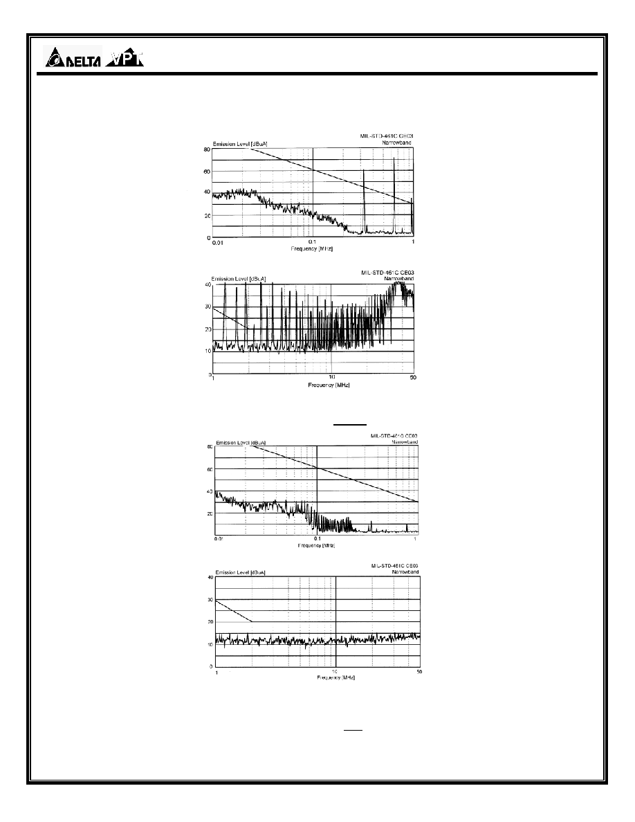
EMI PERFORMANCE CURVES
(T
CASE
= 25∞C, V
IN
= +28V ± 5%, Full Load, Unless Otherwise Specified)
Figure 9
≠ DVTR2800T without EMI Filter
Figure 10
≠ DVTR2800T with EMI Filter
DVTR2800T Series
1X009DSG
9
PACKAGE SPECIFICATIONS (NON-FLANGED, SOLDER SEAL)
TOP VIEW
SIDE VIEW
PIN
FUNCTION
1 28V
IN
2 +V
MAIN
3 OUT
COM
4 -V
AUX
5 +V
AUX
6 CASE
7 CASE
8 INHIBIT
9 SYNC
10 IN
COM
BOTTOM VIEW
Figure 11
≠ Non-Flanged, Solder Seal Tin Plated Package and Pinout (Not Used for /HB or Higher Screened Products)
(Dimensional Limits are ±0.005" Unless Otherwise Stated)

DVTR2800T Series
1X009DSG
10
PACKAGE SPECIFICATIONS (NON-FLANGED, SEAM SEAL)
TOP VIEW
SIDE VIEW
PIN
FUNCTION
1 28V
IN
2 +V
MAIN
3 OUT
COM
4 -V
AUX
5 +V
AUX
6 CASE
7 CASE
8 INHIBIT
9 SYNC
10 IN
COM
BOTTOM VIEW
Figure 12
≠ Non-Flanged, Seam Seal Package and Pinout
(Dimensional Limits are ±0.005" Unless Otherwise Stated)

DVTR2800T Series
1X009DSG
11
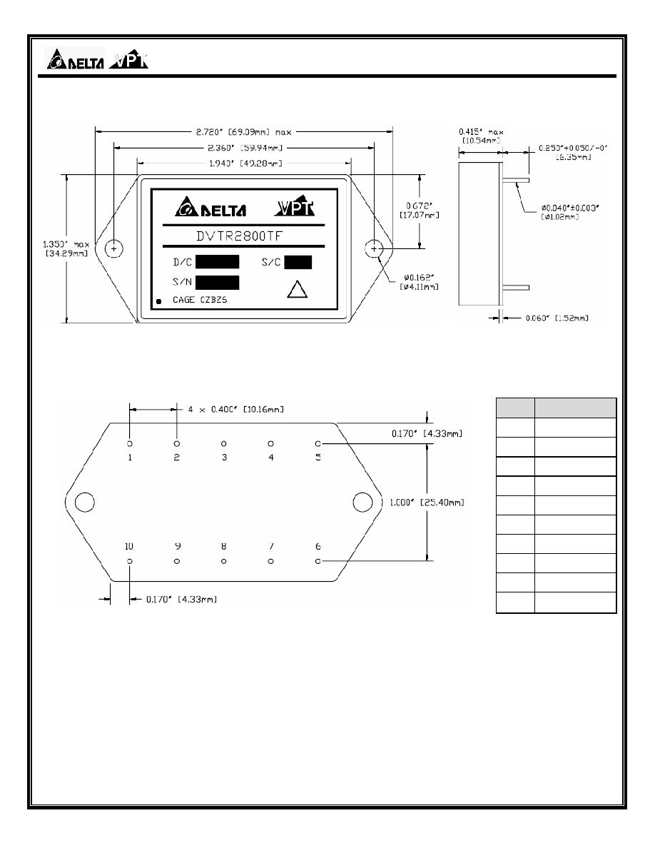
PACKAGE SPECIFICATIONS (FLANGED, SOLDER SEAL)
TOP VIEW
SIDE VIEW
PIN
FUNCTION
1 28V
IN
2 +V
MAIN
3 OUT
COM
4 -V
AUX
5 +V
AUX
6 CASE
7 CASE
8 INHIBIT
9 SYNC
10 IN
COM
BOTTOM VIEW
Figure 13
≠ Flanged, Solder Seal Tin Plated Package and Pinout (Not Used for /HB or Higher Screened Products)
(Dimensional Limits are ±0.005" Unless Otherwise Stated)
DVTR2800T Series
1X009DSG
12
PACKAGE SPECIFICATIONS (FLANGED, SEAM SEAL)
TOP VIEW
SIDE VIEW
PIN
FUNCTION
1 28V
IN
2 +V
MAIN
3 OUT
COM
4 -V
AUX
5 +V
AUX
6 CASE
7 CASE
8 INHIBIT
9 SYNC
10
IN
COM
BOTTOM VIEW
Figure 14
≠ Flanged, Seam Seal Package and Pinout
(Dimensional Limits are ±0.005" Unless Otherwise Stated)
DVTR2800T Series
1X009DSG
13
PACKAGE PIN DESCRIPTION
Pin
Function
Description
1
28V IN
Positive Input Voltage Connection
2
+V MAIN
Positive Main Output Voltage Connection
3 OUT
COM
Output Common Connection
4
-V AUX
Negative Auxiliary Output Voltage Connection
5
+V AUX
Positive Auxiliary Output Voltage Connection
6 CASE
Case
Connection
7 CASE
Case
Connection
8 INHIBIT
Logic Low = Disabled Output. Connecting the inhibit pin to input common causes
converter shutdown.
Logic High = Enabled Output. Unconnected or open collector TTL.
9 SYNC
Synchronization
Signal
10
IN COM
Input Common Connection

DVTR2800T Series
1X009DSG
14
ENVIRONMENTAL SCREENING
(100% Tested Per MIL-STD-883 as referenced to MIL-PRF-38534)
Notes:
1.
100% R&R testing at ≠55∞C, +25∞C, and +125∞C with all test data included in product shipment.
2.
PIND test Certificate of Compliance included in product shipment.
3. Radiographic
test
Certificate of Compliance and film(s) included in product shipment.
Screening
MIL-STD-883
Standard
(No Suffix)
Extended
/ES
HB
/HB
Class H
/H
Class K
/K
Non-
Destructive
Bond Pull
Method 2023
∑
∑
∑
∑
∑
Internal
Visual
Method 2017, 2032
Internal Procedure
∑
∑
∑
∑
∑
Temperature
Cycling
Method 1010, Condition C
Method 1010, -55∞C to 125∞C
∑
∑
∑
∑
Constant
Acceleration
Method 2001, 3000g, Y1 Direction
Method 2001, 500g, Y1 Direction
∑
∑
∑
∑
PIND
Method 2020, Condition A
2
∑
Pre Burn-In
Electrical
100%
at
25∞C
∑
Burn-In
Method 1015, 320 hours at +125∞C
Method 1015, 160 hours at +125∞C
96 hours at +125∞C
24 hours at +125∞C
∑
∑
∑
∑
∑
Final
Electrical
MIL-PRF-38534, Group A
1
100% at 25∞C
∑
∑
∑
∑
∑
Hermeticity
Method 1014, Fine Leak, Condition A
Method 1014, Gross Leak, Condition C
Dip (1 x 10
-3
)
∑
∑
∑
∑
∑
∑
∑
∑
∑
Radiography Method
2012
3
∑
External
Visual
Method 2009
∑
∑
∑
∑
∑
DVTR2800T Series
1X009DSG
15
ORDERING INFORMATION
DVTR
28
5
12
T
F
/HB - XXX
1 2 3 4 5 6 7 8
(1) (2) (3) (4)
Product Series
Nominal Input
Voltage
Main Output Voltage
Auxiliary Output
Voltages
DVTR
28
28 Volts
5
+ 5 Volts
12
15
± 12 Volts
± 15 Volts
(5) (6) (7)
Package Option
Screening Code
1,2
Additional Screening
Code
None
F
Non-
Flanged
Flanged
None
/ES
/HB
/H
/K
Standard
Extended
HB
Class H
Class K
Contact Sales
Notes:
1.
Contact the VPT Inc. Sales Department for
availability of Class H (/H) or Class K (/K) qualified products.
2.
VPT Inc. reserves the right to ship higher screened or SMD products to meet lower screened orders at our
sole discretion unless specifically forbidden by customer contract.
Please contact your sales representative or the VPT Inc. Sales Department for more information
concerning additional environmental screening and testing, different input voltage, output voltage,
power requirement, source inspection, and/or special element evaluation for space or other higher
quality applications.

DVTR2800T Series
1X009DSG
16
SMD (STANDARD MICROCIRCUIT DRAWING) NUMBERS
Standard Microcircuit
Drawing (SMD)
DVTR2800T Series
Similar Part Number
*T.B.D.
DVTR28512T/H
DVTR28512TF/H
*T.B.D.
DVTR28515T/H
DVTR28515TF/H
Do not use the DVTR2800T Series similar part number for SMD product acquisition. It is listed for
reference only. For exact specifications for the SMD product, refer to the SMD drawing. SMD's can be
downloaded from the DSCC website at
http://www.dscc.dla.mil/programs/smcr/
. The SMD number
listed above is for MIL-PRF-38534 Class H screening, standard gold plated lead finish, and no RHA
(Radiation Hardness Assurance) level. Please reference the SMD for other screening levels, lead
finishes, and radiation levels.
CONTACT INFORMATION
To request a quotation or place orders please contact your sales representative or the VPT Inc. Sales
Department at:
Phone
: (425)
353-3010
Fax
:
(425) 353-4030
E-mail
: vptsales@vpt-inc.com
All information contained in this datasheet is believed to be accurate, however, no responsibility is assumed for possible errors
or omissions. The products or specifications contained herein are subject to change without notice.