DS28010 Rev. B-2
1 of 2
10A01-10A07
10A01 - 10A07
10A RECTIFIER
Features
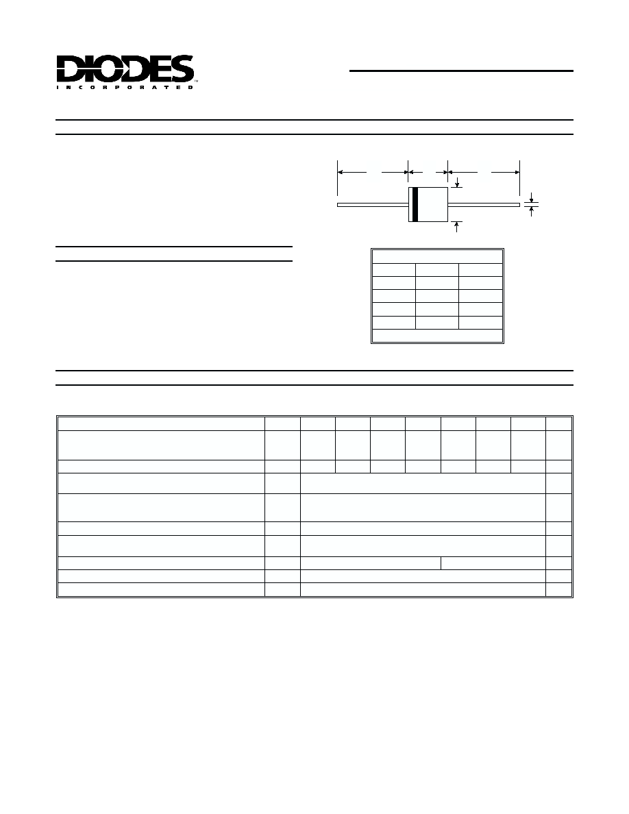
A
A
B
C
D
R-6
Dim
Min
Max
A
25.40
--
B
8.60
9.10
C
1.20
1.30
D
8.60
9.10
All Dimensions in mm
Maximum Ratings and Electrical Characteristics
@ T
A
= 25∞C unless otherwise specified
∑
Diffused Junction
∑
High Current Capability and Low Forward
Voltage Drop
∑
Surge Overload Rating to 600A Peak
∑
Low Reverse Leakage Current
∑
Plastic Material - UL Flammability
Classification 94V-0
Mechanical Data
∑
Case: Molded Plastic
∑
Terminals: Plated Leads Solderable per
MIL-STD-202, Method 208
∑
Polarity: Cathode Band
∑
Weight: 2.1 grams (approx)
∑
Marking: Type Number
Single phase, half wave, 60Hz, resistive or inductive load.
For capacitive load, derate current by 20%.
Characteristic
Symbol 10A01 10A02 10A03 10A04 10A05 10A06 10A07 Unit
Peak Repetitive Reverse Voltage
Working Peak Reverse Voltage
DC Blocking Voltage
V
RRM
V
RWM
V
R
50
100
200
400
600
800
1000
V
RMS Reverse Voltage
V
R(RMS)
35
70
140
280
420
560
700
V
Average Rectified Output Current
(Note 1)
@ T
A
= 50∞C
I
O
10
A
Non-Repetitive Peak Forward Surge Current 8.3ms
single half sine-wave superimposed on rated load
(JEDEC Method)
I
FSM
600
A
Forward Voltage
@ I
F
= 10A
V
FM
1.0
V
10Peak Reverse Current
@T
A
= 25∞C
at Rated DC Blocking Voltage
@ T
A
= 100∞C
I
RM
10
100
µA
Typical Junction Capacitance (Note 2)
C
j
150
80
pF
Typical Thermal Resistance Junction to Ambient
R
qJA
10
K/W
Operating and Storage Temperature Range
T
j,
T
STG
-65 to +150
∞C
Notes:
1. Leads maintained at ambient temperature at a distance of 9.5mm from the case.
2. Measured at 1.0 MHz and applied reverse voltage of 4.0V DC.
DS28010 Rev. B-2
2 of 2
10A01-10A07
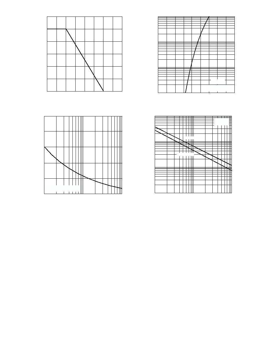
2.0
4.0
6.0
8.0
0
0
I
,
A
VERAGE
RECTIFIED
CURRENT
(A)
(A
V)
TA, AMBIENT TEMPERATURE (∫C)
Fig. 1 Forward Current Derating Curve
12
10
50
100
150
200
I
,
INST
ANT
ANEOUS
FOR
W
ARD
CURRENT
(A)
F
V , INSTANTANEOUS FORWARD VOLTAGE (V)
Fig. 2 Typical Forward Characteristics
F
0.1
1.0
10
100
0
0.4
0.8
1.2
1.6
Pulse Width = 300 ms
2% Duty Cycle
T = 25∫C
j
10
100
1000
1
10
100
C
,
JUNCTION
CAP
ACIT
ANCE
(pF)
j
V , REVERSE VOLTAGE (V)
Fig. 4 Typical Junction Capacitance
R
1.0
T = 25∞C
f = 1MHz
j
10A01 - 10A04
10A05 - 10A07
0
200
400
600
800
1000
1
10
100
I
,
PEAK
FOR
W
ARD
SURGE
CURRENT
(A)
FSM
NUMBER OF CYCLES AT 60 Hz
Fig. 3 Maximum Non-Repetitive Peak Forward Surge Current
8.3ms Single Half Sine-Wave
JEDEC Method