D
S21211 Rev. C-3 1 of 2 DB101-DB107
∑
UL Recognized Component
∑
Ideal for Printed Circuit Board
∑
Glass Passivated Chip Junctions, Surge Overload
Rating of 50A Peak
∑
Simple, Compact Structure for Trouble-free
Performance
∑
Plastic Package - UL Flammability
Classification 94V-0
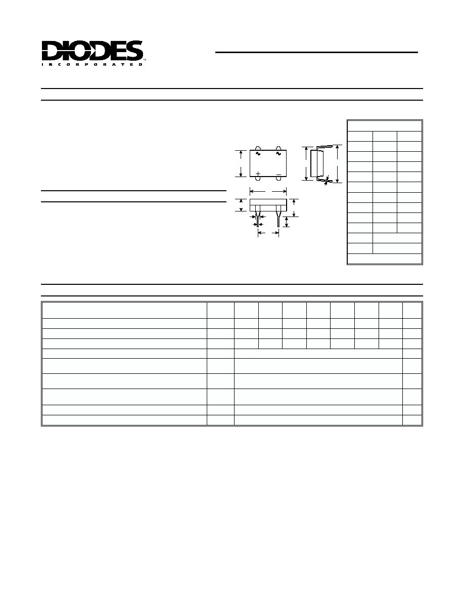
Mechanical Data
Features
∑
Terminals: Tin Plated Leads Solderable per
MIL-STD-202, Method 208
∑
Case: Transfer Molded Epoxy
∑
Mounting Position: Any
∑
Polarity: Polarity Symbols Marked on Body
∑
Approx. Weight: 1.0 grams
Maximum Ratings and Electrical Characteristics
@ T
A
= 25∞C unless otherwise specified
Characteristic
Symbol
DB
101
DB
102
DB
103
DB
104
DB
105
DB
106
DB
107
Unit
Maximum Recurrent Peak Reverse Voltage
V
RRM
50
100
200
400
600
800
1000
V
Maximum RMS Input Voltage
V
RMS
35
70
140
280
420
560
700
V
Maximum DC Blocking Voltage
V
DC
50
100
200
400
600
800
1000
V
Maximum Average Rectified Output Current @ T
A
= 40
∞C
I
(AV)
1.0
A
Peak Forward Surge Current Single Half Sine-wave
Superimposed on Rated Load (JEDEC Method)
I
FSM
50
A
Maximum Instantaneous Forward Voltage drop
per Element at I
F
= 1.0A
V
F
1.1
V
Maximum Reverse DC Current at Rated
@ T
A
= 25
∞C
DC Blocking Voltage per Element
@ T
A
= 100
∞C
I
R
10
1.0
mA
mA
Typical Thermal Resistance (Note 1)
R
q
JA
40
K/W
Storage and Operating Temperature Range
T
J
, T
STG
-55 to +150
∞C
DB101 - DB107
1.0A GLASS PASSIVATED BRIDGE RECTIFIER
DB-1
Dim
Min
Max
A
6.10
6.60
B
7.11
8.13
C
8.13
9.40
D
0.20
0.38
E
-
9.40
G
-
3.30
H
-
5.51
J
2.80
3.68
K
1.02
1.40
L
0.51 Typical
M
5.15 Typical
All Dimensions in mm
D
E
H
J
K
L
M
B
A
C
G
Notes:
1. Thermal resistance from junction to ambient mounted on PC board with 13mm x 13mm copper pads.
2. 60 Hz resistive or inductive load.
3. For capacitive load, derate current by 20%.
D
S21211 Rev. C-3 2 of 2 DB101-DB107
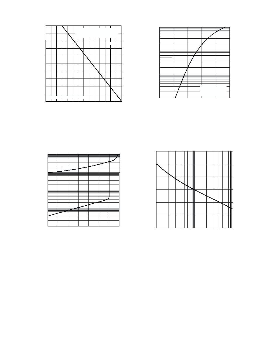
0
0.2
0.4
0.6
0.8
1.0
20
40
60
80
100
120 140
I
,
A
VERAGE
OUTPUT
CURRENT
(A)
AV
T , AMBIENT TEMPERATURE (∫C)
Fig. 1 Maximum Output Rectified Current
A
Mounted on PC board
with 12.7 X 12.7mm Copper pads
Note 1
60 Hz Resistive or Inductive Load
0
10
20
1
10
100
I
,
PEAK
FOR
W
ARD
SURGE
CURRENT
(A)
FSM
NUMBER OF CYCLES AT 60 Hz
Fig. 4 Max Non-Repetitive Peak Forward Surge Current
30
40
50
60
0.01
0.1
1.0
10
100
0
20
40
60
80
100
120 140
IR,
INST
ANT
ANEOUS
REVERSE
CURRENT
(mA)
PERCENT OF RATED PEAK REVERSE VOLTAGE (%)
Fig. 3 Typical Reverse Characteristics
T = 25∫C
J
TJ = 125∞C
0.4
0.6
0.8
0.01
0.1
1.0
10
I
,
INST
ANT
ANEOUS
FOR
W
ARD
CURRENT
(A)
F
V , INSTANTANEOUS FORWARD VOLTAGE (VOLTS)
Fig. 2 Typical Forward Characteristics
F
1.0
1.2
1.4
TJ = 25∫C
Pulse Width = 300µs
2% Duty Cycle