DS30339 Rev. 2 - 2
1 of 3
DDTC (R1-ONLY SERIES) KA
DDTC
(R1-ONLY SERIES)
KA
NPN PRE-BIASED SMALL SIGNAL SC-59
SURFACE MOUNT TRANSISTOR
∑
Epitaxial Planar Die Construction
∑
Complementary PNP Types Available
(DDTA)
∑
Built-In Biasing Resistor, R1 only
Features
Maximum Ratings
@ T
A
= 25
∞C unless otherwise specified
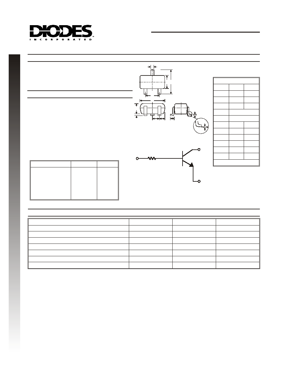
Mechanical Data
∑
Case: SC-59, Molded Plastic
∑
Case material - UL Flammability Rating 94V-0
∑
Moisture sensitivity: Level 1 per J-STD-020A
∑
Terminals: Solderable per MIL-STD-202,
Method 208
∑
Terminal Connections: See Diagram
∑
Marking: Date Code and Marking Code
(See Diagrams & Page 2)
∑
Weight: 0.008 grams (approx.)
∑
Ordering Information (See Page 2)
T
C
U
D
O
R
P
W
E
N
B
R
1
SCHEMATIC DIAGRAM
E
C
P/N
R1 (NOM)
MARKING
DDTC113TKA
DDTC123TKA
DDTC143TKA
DDTC114TKA
DDTC124TKA
DDTC144TKA
DDTC115TKA
DDTC125TKA
1K
W
2.2K
W
4.7K
W
10K
W
22K
W
47K
W
100K
W
200K
W
N01
N03
N07
N12
N16
N19
N23
N25
Characteristic
Symbol
Value
Unit
Collector-Base Voltage
V
CBO
50
V
Collector-Emitter Voltage
V
CEO
50
V
Emitter-Base Voltage
V
EBO
5
V
Collector Current
I
C
(Max)
100
mA
Power Dissipation
P
d
200
mW
Thermal Resistance, Junction to Ambient Air (Note 1)
R
qJA
625
∞C/W
Operating and Storage and Temperature Range
T
j
, T
STG
-55 to +150
∞C
SC-59
Dim
Min
Max
A
0.35
0.50
B
1.50
1.70
C
2.70
3.00
D
0.95
G
1.90
H
2.90
3.10
J
0.013
0.10
K
1.00
1.30
L
0.35
0.55
M
0.10
0.20
a
0
∞
8
∞
All Dimensions in mm
Note:
1. Mounted on FR4 PC Board with recommended pad layout at http://www.diodes.com/datasheets/ap02001.pdf.
A
M
J
L
F
D
B C
H
K
G
B
E
C

DS30339 Rev. 2 - 2
2 of 3
DDTC (R1-ONLY SERIES) KA
Characteristic
Symbol
Min
Typ
Max
Unit
Test Condition
Collector-Base Breakdown Voltage
BV
CBO
50
æ
æ
V
I
C
= 50
mA
Collector-Emitter Breakdown Voltage
BV
CEO
50
æ
æ
V
I
C
= 1mA
Emitter-Base Breakdown Voltage
BV
EBO
5
æ
æ
V
I
E
= 50
mA
Collector Cutoff Current
I
CBO
æ
æ
0.5
mA
V
CB
= 50V
Emitter Cutoff Current
I
EBO
æ
æ
0.5
mA
V
EB
= 4V
Collector-Emitter Saturation Voltage
V
CE(sat)
æ
æ
0.3
V
I
C/
I
B
= 10mA/1mA DDTC113TKA
I
C/
I
B
= 5mA/0.5mA DDTC123TKA
I
C/
I
B
= 2.5mA/.25mA DDTC143TKA
I
C/
I
B
= 1mA/.1mA DDTC114TKA
I
C/
I
B
= 5mA/0.5mA DDTC124TKA
I
C/
I
B
= 2.5mA/.25mA DDTC144TKA
I
C/
I
B
= 1mA/0.1mA DDTC115TKA
I
C/
I
B
= .5mA/.05mA DDTC125TKA
DC Current Transfer Ratio
h
FE
100
250
600
æ
I
C
= 1mA, V
CE
= 5V
Input Resistor (R
1
) Tolerance
DR
1
-30
æ
+30
%
æ
Gain-Bandwidth Product*
f
T
æ
250
æ
MHz
V
CE
= 10V, I
E
= -5mA,
f = 100MHz
Electrical Characteristics
@ T
A
= 25
∞C unless otherwise specified
T
C
U
D
O
R
P
W
E
N
* Transistor - For Reference Only
Month
Jan
Feb
March
Apr
May
Jun
Jul
Aug
Sep
Oct
Nov
Dec
Code
1
2
3
4
5
6
7
8
9
O
N
D
Year
2002
2003
2004
2005
2006
2007
2008
2009
Code
N
P
R
S
T
U
V
W
Date Code Key
XXX = Product Type Marking Code
See Sheet 1 Diagrams
YM = Date Code Marking
Y = Year ex: N = 2002
M = Month ex: 9 = September
XXX
YM
Marking Information
Notes:
2. For Packaging Details, go to our website at http://www.diodes.com/datasheets/ap02007.pdf.
Ordering Information
Device
Packaging
Shipping
DDTC113TKA-7
SC-59
3000/Tape & Reel
DDTC123TKA-7
SC-59
3000/Tape & Reel
DDTC143TKA-7
SC-59
3000/Tape & Reel
DDTC114TKA-7
SC-59
3000/Tape & Reel
DDTC124TKA-7
SC-59
3000/Tape & Reel
DDTC144TKA-7
SC-59
3000/Tape & Reel
DDTC115TKA-7
SC-59
3000/Tape & Reel
DDTC125TKA-7
SC-59
3000/Tape & Reel

DS30339 Rev. 2 - 2
3 of 3
DDTC (R1-ONLY SERIES) KA
T
C
U
D
O
R
P
W
E
N
1
1
10
0
10
20
30
40
50
I , COLLECTOR CURRENT (mA)
C
Fig. 6 Input Voltage vs. Collector Current
V = 0.2
O
V
,
INPUT
V
OL
T
A
GE
(V)
in
-25∞C
25∞C
75∞C
0.01
0.1
1
10
100
0
1
2
3
4
8
9
10
I
,
COLLECT
OR
CURRENT
(mA)
C
V , INPUT VOLTAGE (V)
in
Fig. 5 Collector Current Vs. Input Voltage
-25∞C
5
6
7
75∞C
25∞C
0.001
0
1
2
3
4
0
20
30
C
,
C
AP
A
C
IT
AN
C
E
(
pF
)
OB
V , REVERSE BIAS VOLTAGE (V)
R
Fig. 4 Output Capacitance
10
5
15
25
I = 0mA
E
10
1000
100
1
1
10
100
hFE,
D
C
CURRENT
GAIN
(NORMALIZED)
I , COLLECTOR CURRENT (mA)
C
Fig. 3 DC Current Gain
V = 10
CE
75∞C
-25∞C
25∞C
0.001
0.01
0.1
1
0
10
20
30
40
50
V
,
MAXIMUM
C
OLLECT
OR
VOL
T
AGE
(V)
CE(SA
T
)
I , COLLECTOR CURRENT (mA)
C
Fig. 2 V
vs. I
CE(SAT)
C
I /I = 10
C B
-25∞C
75∞C
25∞C
-50
0
50
100
150
250
200
150
50
100
0
T , AMBIENT TEMPERATURE (∞C)
A
Fig. 1 Derating Curve
P
,
POWER
D
ISSIP
A
TION
(MILLIW
A
TTS)
D
TYPICAL CURVES - DDTC114TKA