DS30398 Rev. 2 - 2
1 of 3
DDTD (LO-R1) U
www.diodes.com
„
Diodes Incorporated
DDTD (LO-R1) U
NPN PRE-BIASED 500 mA SOT-323
SURFACE MOUNT TRANSISTOR
∑
Epitaxial Planar Die Construction
∑
Complementary PNP Types Available
(DDTB)
∑
Built-In Biasing Resistors
∑
Lead Free Product
Features
Maximum Ratings
@ T
A
= 25
∞C unless otherwise specified
A
M
J
L
E
D
B C
H
K
G
IN
GND
OUT
3
2
1
Mechanical Data
∑
Case: SOT-323, Molded Plastic
∑
Case material - UL Flammability Rating 94V-0
∑
Moisture sensitivity: Level 1 per J-STD-020A
∑
Terminals: Finish - Matte Tin (Note 1)
Solderable per MIL-STD-202, Method 208
∑
Terminal Connections: See Diagram
∑
Marking: Date Code and Marking Code
(See Diagrams & Page 2)
∑
Weight: 0.006 grams (approx.)
∑
Ordering Information (See Page 2)
T
C
U
D
O
R
P
W
E
N
(2) IN
R
1
R
2
GND (1)
OUT (3)
SOT-323
Dim
Min
Max
A
0.25
0.40
B
1.15
1.35
C
2.00
2.20
D
0.65 Nominal
E
0.30
0.40
G
1.20
1.40
H
1.80
2.20
J
0.0
0.10
K
0.90
1.00
L
0.25
0.40
M
0.10
0.18
a
0
∞
8
∞
All Dimensions in mm
Characteristic
Symbol
Value
Unit
Supply Voltage, (3) to (1)
V
CC
50
V
Input Voltage, (2) to (1)
DDTD122LU
DDTD142JU
V
IN
-5 to +6
-5 to +6
V
Input Voltage, (1) to (2) DDTD122TU
DDTD142TU
V
EBO (MAX)
5
V
Output Current All
I
C
500
mA
Power Dissipation (Note 2)
P
d
200
mW
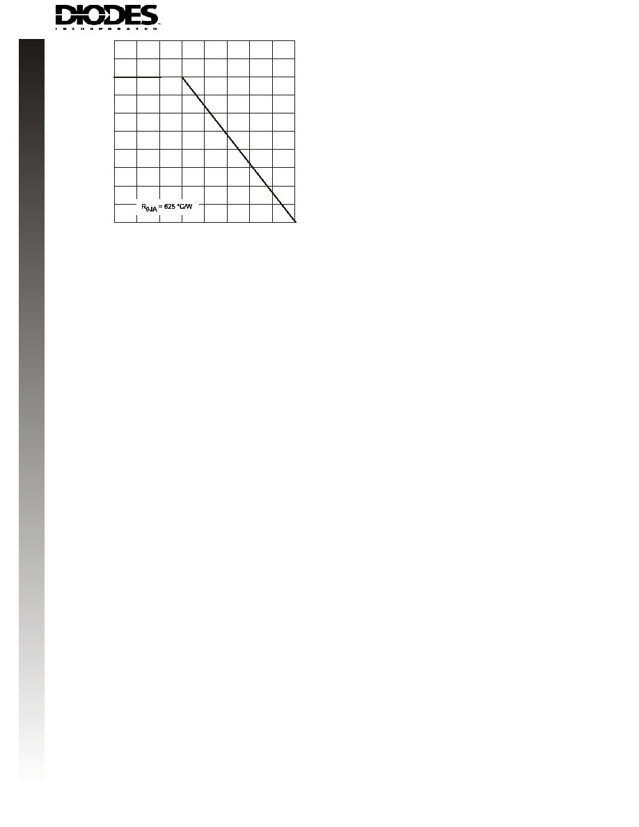
Thermal Resistance, Junction to Ambient Air (Note 2)
R
qJA
625
∞C/W
Operating and Storage and Temperature Range
T
j
, T
STG
-55 to +150
∞C
P/N
R1 (NOM) R2 (NOM)
MARKING
DDTD122LU
DDTD142JU
DDTD122TU
DDTD142TU
0.22K
W
0.47K
W
0.22K
W
0.47K
W
10K
W
10K
W
OPEN
OPEN
N75
N76
N77
N78
Note: 1. If lead-bearing terminal plating is required, please contact your Diodes Inc. sales representative for availability and minimum
order details.
2. Mounted on FR4 PC Board with recommended pad layout at http://www.diodes.com/datasheets/ap02001.pdf.
DS30398 Rev. 2 - 2
2 of 3
DDTD (LO-R1) U
www.diodes.com
* Transistor - For Reference Only
Electrical Characteristics R1, R2 Types
@ T
A
= 25
∞C unless otherwise specified
Characteristic
Symbol
Min
Typ
Max
Unit
Test Condition
Input Voltage
DDTD122LU
DDTD142JU
V
l(off)
0.3
0.3
æ
æ
V
V
CC
= 5V, I
O
= 100
mA
DDTD122LU
DDTD142JU
V
l(on)
æ
æ
2.0
2.0
V
V
O
= 0.3V, I
O
= 20mA
V
O
= 0.3V, I
O
= 20mA
Output Voltage
V
O(on)
æ
æ
0.3V
V
I
O
/I
l
= 50mA/2.5mA
Input Current
DDTD122LU
DDTD142JU
I
l
æ
æ
28
13
mA
V
I
= 5V
Output Current
I
O(off)
æ
æ
0.5
mA
V
CC
= 50V, V
I
= 0V
DC Current Gain
DDTD122LU
DDTD142JU
G
l
56
56
æ
æ
æ
V
O
= 5V, I
O
= 50mA
Gain-Bandwidth Product*
f
T
æ
200
æ
MHz
V
CE
= 10V, I
E
= 5mA,
f = 100MHz
Electrical Characteristics R1-Only, R2-Only Types
@ T
A
= 25
∞C unless otherwise specified
* Transistor - For Reference Only
Characteristic
Symbol
Min
Typ
Max
Unit
Test Condition
Collector-Base Breakdown Voltage
BV
CBO
50
æ
æ
V
I
C
= 50
mA
Collector-Emitter Breakdown Voltage
BV
CEO
40
æ
æ
V
I
C
= 1mA
Emitter-Base Breakdown Voltage DDTD122TU
DDTD142TU
BV
EBO
5
æ
æ
V
I
E
= 50
mA
I
E
= 50
mA
Collector Cutoff Current
I
CBO
æ
æ
0.5
mA
V
CB
= 50V
Emitter Cutoff Current
DDTD122TU
DDTD142TU
I
EBO
æ
æ
æ
0.5
0.5
mA
V
EB
= 4V
Collector-Emitter Saturation Voltage
V
CE(sat)
æ
æ
0.3
V
I
C
= 50mA, I
B
= 2.5mA
DC Current Transfer Ratio
DDTD122TU
DDTD142TU
h
FE
100
100
250
250
600
600
æ
I
C
= 5mA, V
CE
= 5V
Gain-Bandwidth Product*
f
T
æ
200
æ
MHz
V
CE
= 10V, I
E
= -5mA,
f = 100MHz
Ordering Information
Device
Packaging
Shipping
DDTD122LU-7
SOT-323
3000/Tape & Reel
DDTD142JU-7
SOT-323
3000/Tape & Reel
DDTD122TU-7
SOT-323
3000/Tape & Reel
DDTD142TU-7
SOT-323
3000/Tape & Reel
Marking Information
XXX
YM
XXX = Product Type Marking Code
See Sheet 1 Diagrams
YM = Date Code Marking
Y = Year ex: P = 2003
M = Month ex: 9 = September
Date Code Key
Year
2002
2003
2004
2005
2006
2007
2008
2009
Code
N
P
R
S
T
U
V
W
Month
Jan
Feb
March
Apr
May
Jun
Jul
Aug
Sep
Oct
Nov
Dec
Code
1
2
3
4
5
6
7
8
9
O
N
D
(Note 2)
Notes: 1. If lead-bearing terminal plating is required, please contact your Diodes Inc. sales representative for availability and minimum
order details.
3. For Packaging Details, go to our website at http://www.diodes.com/datasheets/ap02007.pdf.
T
C
U
D
O
R
P
W
E
N