e
3
DS30518 Rev. 1 - 1
1 of 3
DFLS230
PowerDI is a trademark of Diodes Incorporated.
www.diodes.com
„
Diodes Incorporated
DFLS230
2.0A SURFACE MOUNT SCHOTTKY BARRIER RECTIFIER
PowerDI
‰
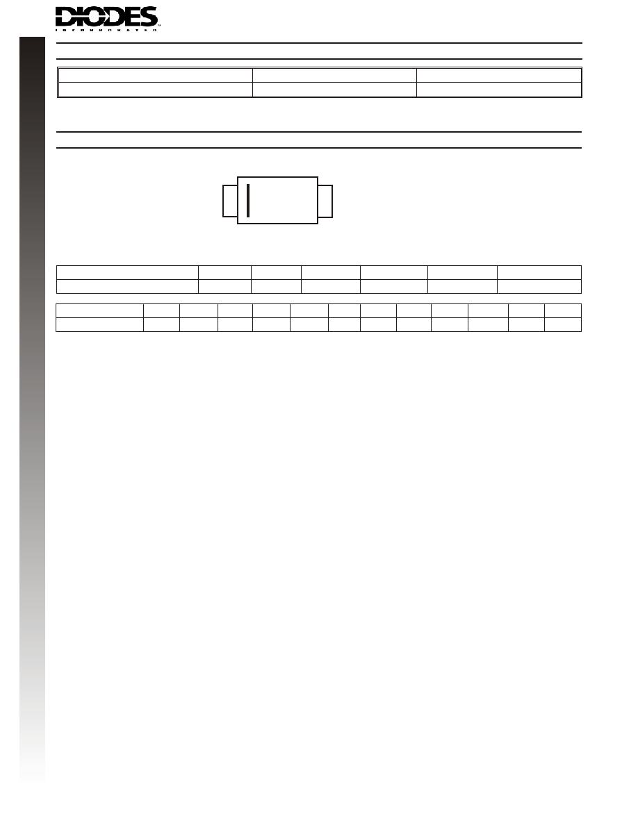
123
B
A
A
C
E
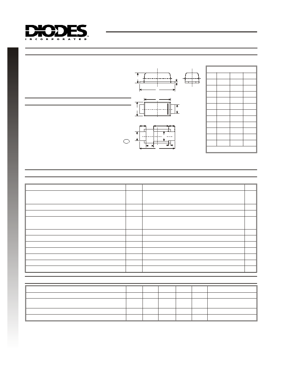
L4
L
L1
E
H
D
L3
L2
L
Maximum Ratings
@ T
A
= 25
∞C unless otherwise specified
∑
Guard Ring Die Construction for
Transient Protection
∑
Low Power Loss, High Efficiency
∑
High Surge Capability
∑
High Current Capability and Low Forward Voltage Drop
∑
Lead Free Finish, RoHS Compliant (Note 5)
∑
"Green" Molding Compound (No Br, Sb)
Mechanical Data
Single phase, half wave, 60Hz, resistive or inductive load. For capacitive load, derate current by 20%.
Characteristic
Symbol
Value
Unit
Peak Repetitive Reverse Voltage
Working Peak Reverse Voltage
DC Blocking Voltage
V
RRM
V
RWM
V
R
30
V
RMS Reverse Voltage
V
R(RMS)
21
V
Average Forward Current @ T
T
= 120∞C
I
F(AV)
2.0
A
Non-Repetitive Peak Forward Surge Current 8.3ms
single half sine-wave superimposed on rated load
(JEDEC Method)
I
FSM
22
A
Power Dissipation (Note 1)
P
D
1.67
W
Power Dissipation (Note 2)
P
D
556
mW
Thermal Resistance Junction to Ambient (Note 1)
R
qJA
60
∞C/W
Thermal Resistance Junction to Ambient (Note 2)
R
qJA
180
∞C/W
Thermal Resistance Junction to Soldering (Note 3)
R
qJS
10
∞C/W
Operating Temperature Range
T
j
-55 to +125
∞C
Storage Temperature Range
T
STG
-55 to +150
∞C
∑
Case: PowerDI
‰
123
∑
Case Material: Molded Plastic, "Green" Molding Compound.
UL Flammability Classification Rating 94V-0
∑
Moisture sensitivity: Level 1 per J-STD-020C
∑
Terminal Connections: Cathode Band
∑
Terminals: Finish ≠ Matte Tin annealed over Copper
leadframe. Solderable per MIL-STD-202, Method 208
∑
Marking & Type Code Information: See Last Page
∑
Weight: 0.01 grams (approx.)
∑
Ordering Information: See Last Page
T
C
U
D
O
R
P
W
E
N
Electrical Characteristics
@ T
A
= 25
∞C unless otherwise specified
Characteristic
Symbol
Min
Typ
Max
Unit
Test Condition
Reverse Breakdown Voltage (Note 4)
V
(BR)R
æ
æ
æ
V
I
R
= 1.5mA
Forward Voltage (Note 4)
V
F
æ
æ
0.36
0.4
0.42
0.49
V
I
F
= 1.0A
I
F
= 2.0A
Leakage Current (Note 4)
I
R
æ
0.15
1.0
mA
V
R
= 30V, T
A
= 25
∞C
Total Capacitance
C
T
æ
75
æ
pF
V
R
= 10V, f = 1.0MHz
Features
Notes: 1. Part mounted on 50.8mm X 50.8mm GETEK board with 25.4mm X 25.4mm copper pad, 25% anode, 75% cathode.
2. Part mounted on FR-4 board with 1.8mm X 2.5mm cathode and 1.8mm X 1.2mm anode, 1 oz. copper pads.
3. Theoretical R
qJS
calculated from the top center of the die straight down to the PCB cathode tab solder junction.
4. Short duration pulse test to minimize self-heating effect.
5. RoHS revision 13.2.2003. Glass and High Temperature Solder Exemptions Applied, see EU Directive Annex Notes 5 and 7.
PowerDI
‰
123
Dim
Min
Max
Typ
A
3.50
3.90
3.70
B
2.60
3.00
2.80
C
1.63
1.93
1.78
D
0.93
1.00
0.98
E
0.85
1.25
1.00
H
0.15
0.25
0.20
L
0.45
0.85
0.65
L1
--
--
1.35
L2
--
--
1.10
L3
--
--
0.20
L4
0.90
1.30
1.05
All Dimensions in mm
SPICE MODEL: DFLS230
DS30518 Rev. 1 - 1
2 of 3
DFLS230
PowerDI is a trademark of Diodes Incorporated.
www.diodes.com
T
C
U
O
R
P
W
E
N
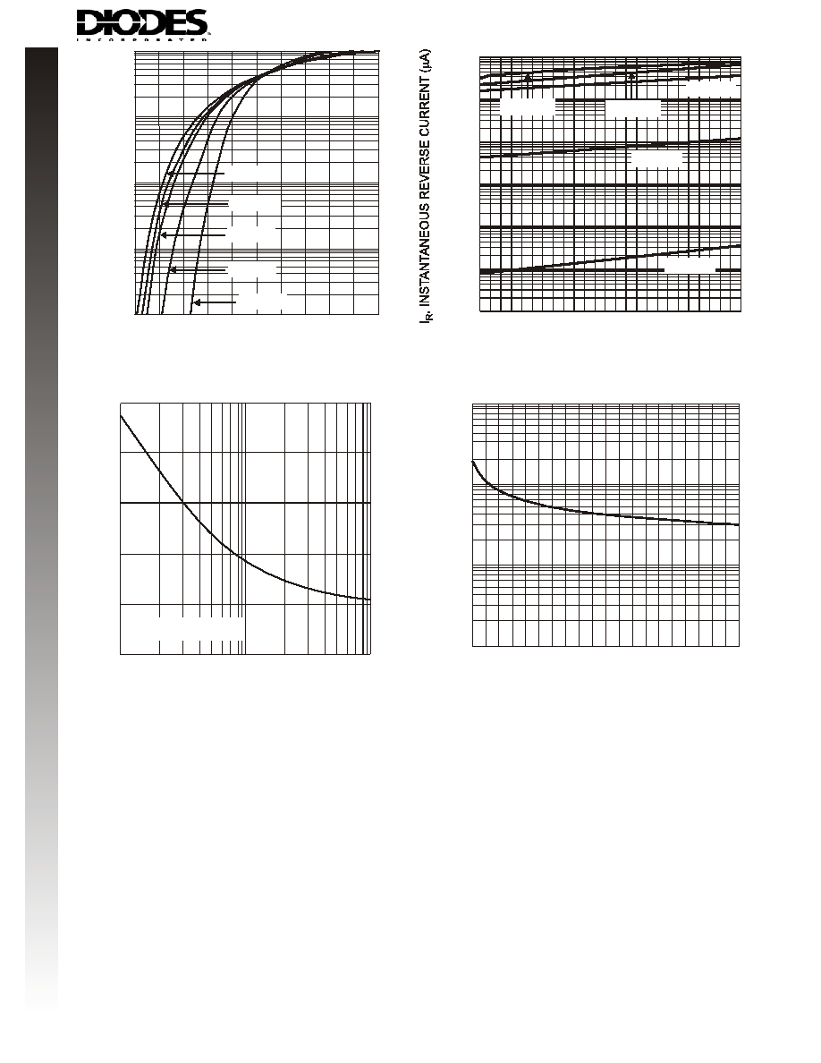
0.001
0.01
10
1
0.1
0.2
0
0.4
0.6
0.8
1.0
I
,
INST
ANT
A
NEOUS
FOR
W
A
RD
CURRENT
(A)
F
V , INSTANTANEOUS FORWARD VOLTAGE (V)
F
Fig. 1, Typical Forward Characteristics
T = 100 C
A
∞
T = 125 C
A
∞
T = 85 C
A
∞
T = 25 C
A
∞
T = -40 C
A
∞
.1
.01
1
10
100
1000
10,000
5
10
15
20
25
30
V , INSTANTANEOUS REVERSE VOLTAGE (V)
R
Fig. 2, Typical Reverse Characteristics
T = 100 C
A
∞
T = 125 C
A
∞
T = 85 C
A
∞
T = 25 C
A
∞
T = -40 C
A
∞
1
10
100
1000
0
10
15
20
C,
T
O
T
A
L
C
AP
ACIT
ANCE
(pF)
T
V , REVERSE VOLTAGE (V)
R
Fig. 4, Typical Total Capacitance
5
0
5
10
15
20
25
1
10
100
I
,
PEAK
F
O
R
W
ARD
S
URGE
CURRENT
(
A)
FSM
NUMBER OF CYCLES AT 60 Hz
Fig. 3, Maximum Non-Repetitive Peak Forward Surge Current
8.3ms Single Half Sine-Wave
JEDEC Method