e
3
DS30581 Rev. 3 - 2
1 of 4
DFLT5V0A - DFLT51A
PowerDI is a trademark of Diodes Incorporated.
www.diodes.com
„
Diodes Incorporated
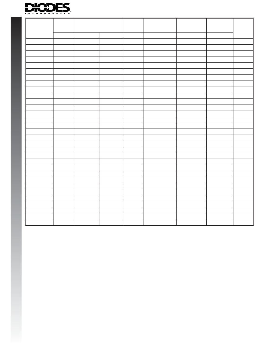
Maximum Ratings
@ T
A
= 25
∞C unless otherwise specified
Characteristic
Symbol
Value
Unit
Peak Pulse Power Dissipation (Note 1) 10/1000
ms
(Note 2) 8/20
ms
P
PK
225
1125
W
Peak Forward Surge Current, 8.3ms Single Half Sine Wave
I
FSM
50
A
Instantaneous Forward Voltage
@ I
PP
= 12A
(Note 5)
V
F
3.5
V
Operating Temperature Range
T
j
-65 to +150
∞C
Storage Temperature Range
T
STG
-65 to +150
∞C
∑
225W Peak Pulse Power Dissipation (10
ms x 1000ms
waveform)
∑
5.0V - 51V Standoff Voltages
∑
Excellent Clamping Capability
∑
Lead Free Finish, RoHS Compliant (Note 6)
∑
"Green" Molding Compound (No Br, Sb)
∑
Qualified to AEC-Q101 Standards for High Reliability
Mechanical Data
Notes: 1. Non-Repetitive current pulse as shown in figure 3 and derated above T
A
= 25
∞C as per figure 1.
2. Non-Repetitive current pulse as shown in figure 5 and derated above T
A
= 25
∞C as per figure 1.
3. Device mounted on 1"x1", FR-4 PCB; 2 oz. Cu pad layout as shown on Diodes Inc. suggested pad layout document AP02001.pdf.
4. Theoretical R
qJS
calculated from the top center of the die straight down to the PCB/cathode tab solder junction.
5. 1/2 sine wave (or equivalent square wave), pulse width = 8.3ms, duty cycle = 4 pulses/minute maximum.
6. RoHS revision 13.2.2003. Glass and High Temperature Solder Exemptions Applied, see
EU Directive Annex Notes 5 and 7.
B
A
A
C
E
L4
L
L1
E
H
D
L3
L2
NEW
P
RODUCT
DFLT5V0A - DFLT51A
225W SURFACE MOUNT TRANSIENT VOLTAGE SUPPRESSOR
PowerDI
‰
123
Features
∑
Case: PowerDI‰123
∑
Case Material: Molded Plastic, "Green" Molding
Compound. UL Flammability Classification Rating
94V-0
∑
Moisture Sensitivity: Level 1 per J-STD-020C
∑
Terminal Connections: Cathode Band
∑
Terminals: Finish
æ Matte Tin annealed over Copper
leadframe. Solderable per MIL-STD-202,
Method 208
∑
Marking & Type Code Information: See Last Page
∑
Ordering Information: See Last Page
∑
Weight: 0.01 grams (approximate)
Characteristic
Symbol
Value
Unit
DC Steady-State Power Dissipation (Note 3)
P
D
1.0
W
Thermal Resistance, Junction to Ambient (Note 3)
R
qJA
125
∞C/W
Thermal Resistance, Junction to Soldering Point (Note 4)
R
qJS
6
∞C/W
Thermal Characteristics
@ T
A
= 25∞C unless otherwise specified
PowerDI
‰
123
Dim
Min
Max
Typ
A
3.50
3.90
3.70
B
2.60
3.00
2.80
C
1.63
1.93
1.78
D
0.93
1.00
0.98
E
0.85
1.25
1.00
H
0.15
0.25
0.20
L
0.45
0.85
0.65
L1
--
--
1.35
L2
--
--
1.10
L3
--
--
0.20
L4
0.90
1.30
1.05
All Dimensions in mm

DS30581 Rev. 3 - 2
3 of 4
DFLT5V0A - DFLT51A
PowerDI is a trademark of Diodes Incorporated.
www.diodes.com
10 X 1000 Waveform
as defined by REA
0
25
50
75
100
125
150 175 200
100
75
50
25
0
T , AMBIENT TEMPERATURE ( C)
Fig. 1 Pulse Derating Curve
A
∞
PEAK
PULSE
D
ERA
TING
I
N
%
O
F
PEAK
POWER
O
R
CURRENT
0.1
1.0
0.1
10
100
t , PULSE WIDTH (ms)
Fig. 5 Pulse Rating Curve
p
1.0
10
1000
10000
T = 25 C
j
∞
P
,
PEAK
PULSE
P
O
WER
(kW)
PK
100
Non Repetitive
Pulse Waveform
Shown in Fig. 4
0
t, TIME ( s)
Fig. 4 Pulse Waveform
m
20
40
60
100
50
0
Peak Value I
pp
Half Value I /2
pp
8x20 Waveform
as defined by R.E.A.
t
p
I
,
PEAK
PULSE
CURRENT
(%I
)
Pp
p
P
NEW
P
RODUCT
0
1
2
3
100
50
0
I
,
PEAK
PULSE
CURRENT
(%I
)
Pp
p
P
Peak Value I
pp
Half Value I /2
pp
10 X 1000 Waveform
as defined by R.E.A.
t
p
t, TIME (ms)
Fig. 3 Pulse Waveform
0
0.2
0.4
0.6
0
25
50
75
100
125
150
P
S
TEADY
S
T
A
TE
POWER
D
ISSIP
A
TION
(W)
(A
V),
T , TERMINAL TEMPERATURE ( C)
Fig. 2 Steady State Power Derating Curve
T
∞
1.0
0.8
1.2
TOTAL CAPACITANCE
Fig. 6 V
(V)
RWM
0
200
400
600
800
1000
1200
1400
1600
0
10
20
30
40
50
60
T
O
T
A
L
C
AP
ACIT
ANCE
(pF)
V = 0V
f = 1MHz
R

DS30581 Rev. 3 - 2
4 of 4
DFLT5V0A - DFLT51A
PowerDI is a trademark of Diodes Incorporated.
www.diodes.com
Marking Information
Ordering Information
Device
Packaging
Shipping
DFLTxxxA-7*
PowerDI
‰
123
3000/Tape & Reel
Notes:
8. For Packaging Details, go to our website at http://www.diodes.com/datasheets/ap02007.pdf.
* Add "-7" to the appropriate type number in Table 1 on page 2. Example: 10V reverse standoff device = DFLT10A-7.
(Note 8)
NEW
P
RODUCT
Year
2004
2005
2006
2007
2008
2009
Code
R
S
T
U
V
W
Month
Jan
Feb
March
Apr
May
Jun
Jul
Aug
Sep
Oct
Nov
Dec
Code
1
2
3
4
5
6
7
8
9
O
N
D
Date Code Key
FXX = Product Type Marking Code (See Marking Codes on Page 2)
YM = Date Code Marking
Y = Year (ex: R = 2004)
M = Month (ex: 9 = September)
FXX
YM
IMPORTANT NOTICE
LIFE SUPPORT
www.diodes.com
Diodes, Inc. and its subsidiaries reserve the right to make changes without further notice to any product herein to make corrections, modifications, enhance-
ments, improvements, or other changes. Diodes, Inc. does not assume any liability arising out of the application or use of any product described herein;
neither does it convey any license under its patent rights, nor the rights of others. The user of products in such applications shall assume all risks of such
use and will agree to hold Diodes Incorporated and all the companies whose products are represented on our website, harmless against all damages.
The products located on our website at
are not recommended for use in life support systems where a failure or malfunction of the
component may directly threaten life or cause injury without the expressed written approval of Diodes Incorporated.