1 04-02-050A
Commercial/Industrial
PA7572 PEEL ArrayTM
Programmable Electrically Erasable Logic Array
Versatile Logic Array Architecture
- 24 I/Os, 14 inputs, 60 registers/latches
- Up to 72 logic cell output functions
- PLA structure with true product-term sharing
- Logic functions and registers can be I/O-buried
High-Speed Commercial and Industrial Versions
- As fast as 13ns/20ns (tpdi/tpdx), 66.6MHz (f
MAX
)
-
Industrial grade available for 4.5 to 5.5V V
CC
and -40
to +85 ∞C temperatures
Ideal for Combinatorial, Synchronous and
Asynchronous Logic Applications
- Integration of multiple PLDs and random logic
- Buried counters, complex state-machines
- Comparators, decoders, other wide-gate functions
CMOS Electrically Erasable Technology
- Reprogrammable in 40-pin DIP,
44-pin PLCC and TQFP packages
Flexible Logic Cell
- Up to 3 output functions per logic cell
- D,T and JK registers with special features
- Independent or global clocks, resets, presets,
clock polarity and output enables
- Sum-of-products logic for output enables
Development and Programmer Support
- ICT PLACE Development Software
- Fitters for ABEL, CUPL and other software
- Programming support by popular third-party
programmers
General Description
The PA7572 is a member of the Programmable Electrically
Erasable Logic (PEELTM) Array family based on ICT's
CMOS EEPROM technology. PEELTM Arrays free
designers from the limitations of ordinary PLDs by
providing the architectural flexibility and speed needed for
today's programmable logic designs. The PA7572 offers a
versatile logic array architecture with 24 I/O pins, 14 input
pins and 60 registers/latches (24 buried logic cells, 12 input
registers/latches, 24 buried I/O registers/latches). Its logic
array implements 100 sum-of-products logic functions
divided into two groups each serving 12 logic cells. Each
group shares half (60) of the 120 product-terms available.
The PA7572's logic and I/O cells (LCCs, IOCs) are
extremely flexible with up to three output functions per cell
(a total of 72 for all 24 logic cells). Cells are configurable as
D, T, and JK registers with independent or global clocks,
resets, presets, clock polarity, and other features, making
the PA7572 suitable for a variety of combinatorial,
synchronous and asynchronous logic applications. The
PA7572 supports speeds as fast as 13ns/20ns (tpdi/tpdx)
and 66.6MHz (f
MAX
) at moderate power consumption
140mA (100mA typical). Packaging includes 40-pin DIP
and 44-pin PLCC (see Figure 1). ICT and popular third-
party development tool manufacturers provide
development and programming support for the PA7572.
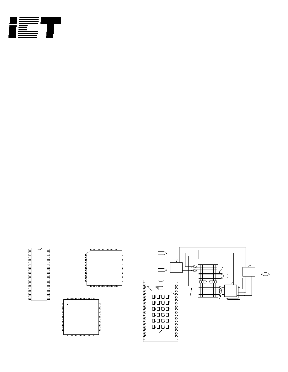
Figure 1. Pin Configuration
08-15 -0 01A
D IP (6 0 0 m il)
I/C LK1
1
I
2
I
3
I
4
I/O
5
I/O
6
I/O
7
I/O
8
I/O
9
I/O
10
I/O
11
I/O
12
VC C
40
I
39
I
38
I
37
I/O
36
I/O
35
I/O
34
I/O
33
I/O
32
I/O
31
I/O
30
I/O
29
I/O
13
I/O
14
I/O
15
I/O
16
I
17
I
18
I
19
G N D
20
I/O
28
I/O
27
I/O
26
I/O
25
I
24
I
23
I
22
I/C LK2
21
7
I/O
8
I/O
9
I/O
10
I/O
11
I/O
12
I/O
13
I/O
18
I/O
19
I
20
I
21
I
22
GN
D
23
GN
D
24
I/C
L
K
2
4
I
3
I
2
I/C
L
K
1
1
VC
C
44
VC
C
43
I
42
I
P L C C
39
G N D
38
I/O
37
I/O
36
I/O
35
I/O
34
I/O
33
I/O
6
I/O
5
I
14
I/O
15
I/O
16
I/O
17
G N D
25
I
26
I
27
I
28
I/O
32
I/O
31
I/O
30
I/O
29
I/O
41
I
40
I/O
1
I/O
2
I/O
3
I/O
4
I/O
5
I/O
6
I/O
7
I/O
12
I/O
13
I
14
I
15
I
16
GN
D
17
GN
D
18
I/C
L
K
2
42
I
41
I
40
I/C
L
K
1
39
VC
C
38
VC
C
37
I
36
I
T Q F P
33
G N D
32
I/O
31
I/O
30
I/O
29
I/O
28
I/O
27
I/O
44
I/O
43
I
8
I/O
9
I/O
10
I/O
11
G N D
19
I
20
I
21
I
22
I/O
26
I/O
25
I/O
24
I/O
23
I/O
35
I
34
I/O
Figure 2. Block Diagram
In p ut
C e lls
(IN C )
1 2 In p u t P ins
2 Inp u t/
G lo b a l C lo c k P in s
G lo b a l
C e lls
2
1 2
I/O
C e lls
(IO C )
L o gic
C o n tro l
C e lls
(L C C )
2 4
2 4
2 4
2 4
A
B
C
D
1 2 4 (6 2 X 2)
A rr ay In p u ts
tr ue an d
c o m p lem e n t
B u rie d
lo g ic
4 s um te rm s
5 p ro d u c t te rm s
fo r G lob a l C e lls
2 4 L o gic C o n tro l C e lls
u p to 3 o utp ut fun c tio ns pe r c e ll
(7 2 tota l o u tp u t fu nc tio n s
p o s s ib le )
L o g ic
fu n c tio n s
to I/O c e lls
2 4 I/O P ins
9 6 s u m ter m s
(fou r p er L C C )
Lo gic
A rray
P A 7572
I
I
I
I/O
I/O
I/O
I/O
I/O
I/O
I
I
I
I
I
I
I/O
I/O
I/O
I/O
I/O
I/O
I
I
I
V C C
I/CLK 2
G N D
I/CLK
I/O
I/O
I/O
I/O
I/O
I/O
G lobal C ells
Input C ells
I/O Cells
I/O
I/O
I/O
I/O
I/O
I/O
Logic C ontrol Cells
08-15-002A
2 04-02-050A
Commercial/Industrial
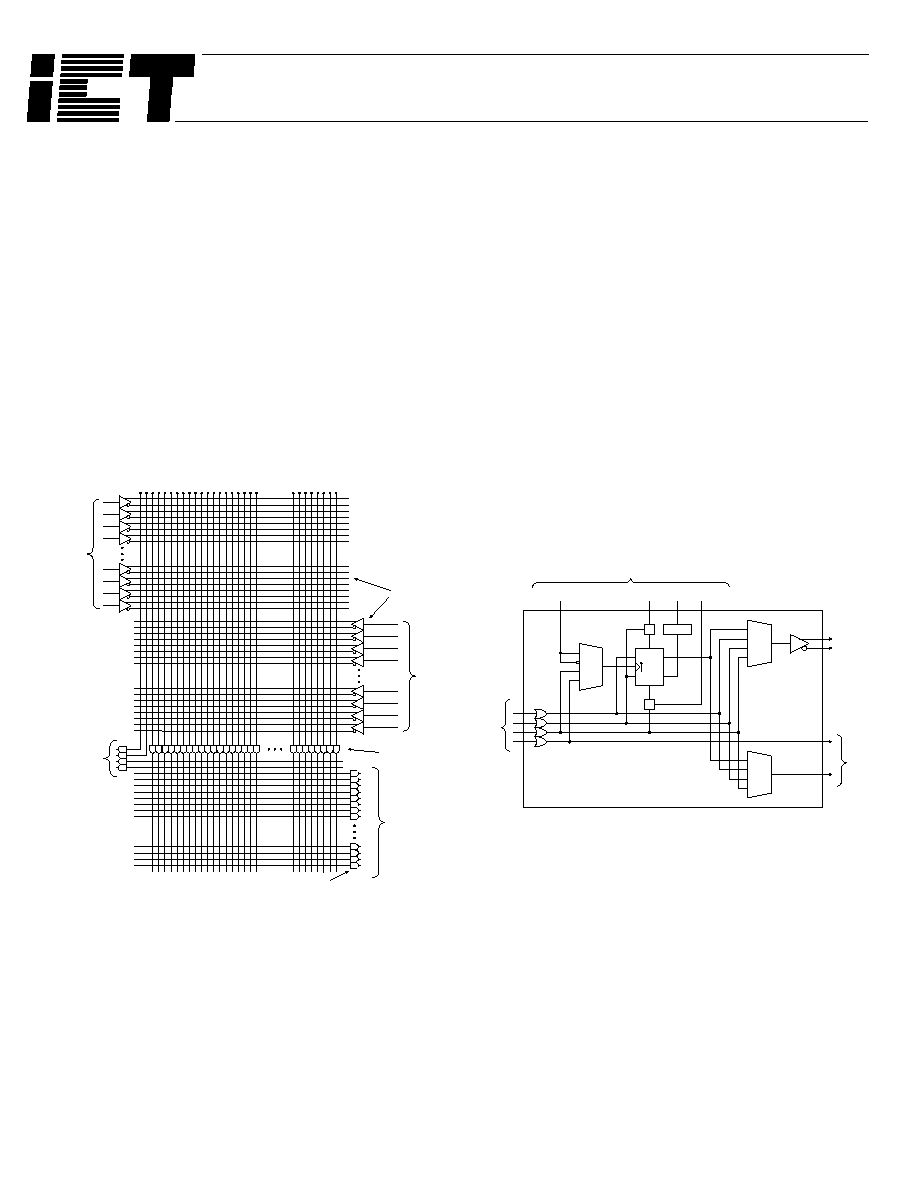
Inside the Logic Array
The heart of the PEELTM Array architecture is based on a
logic array structure similar to that of a PLA (programmable
AND, programmable OR). The logic array implements all
logic functions and provides interconnection and control of
the cells. In the PA7572 PEELTM Array, 62 inputs are
available into the array from the I/O cells, inputs cells and
input/global-clock pins.
All inputs provide both true and complement signals, which
can be programmed to any product term in the array. The
PA7572 PEELTM Arrays contains 124 product terms. All
product terms (with the exception of certain ones fed to the
global cells) can be programmably connected to any of the
sum-terms of the logic control cells (four sum-terms per
logic control cell). Product-terms and sum-terms are also
routed to the global cells for control purposes. Figure 3
shows a detailed view of the logic array structure.
F rom
IO C ells
(IO C ,IN C ,
I/C LK)
F rom
Logic
C ontrol
C ells
(LC C )
T o
G lobal
C ells
62 A rray Inputs
125 P roduct
T erm s
T o
Logic C ontrol
C ells
(LC C )
100 S um Term s
P A 757 2 Log ic A rray
0 8-15 -0 0 3A
Figure 3. PA7572 Logic Array
True Product-Term Sharing
The PEELTM logic array provides several advantages over
common PLD logic arrays. First, it allows for true product-
term sharing, not simply product-term steering, as com-
monly found in other CPLDs. Product term sharing ensures
that product-terms are used where they are needed and
not left unutilized or duplicated. Secondly, the sum-of-
products functions provided to the logic cells can be used for
clocks, resets, presets and output enables instead of just
simple product-term control.
The PEELTM logic array can also implement logic functions
with many product terms within a single-level delay. For
example a 16-bit comparator needs 32 shared product terms
to implement 16 exclusive-OR functions. The PEELTM logic
array easily handles this in a single level delay. Other
PLDs/CPLDs either run out of product-terms or require
expanders or additional logic levels that often slow
performance and skew timing.
Logic Control Cell (LCC)
Logic Control Cells (LCC) are used to allocate and control the
logic functions created in the logic array. Each LCC has four
primary inputs and three outputs. The inputs to each LCC are
complete sum-of-product logic functions from the array, which
can be used to implement combinatorial and sequential logic
functions, and to control LCC registers and I/O cell output
enables.
A
B
C
D
R E G
D,T,J
K
R
P
Q
M U X
S ys tem C lock
P res et
R eset
On /O ff
R egT ype
From G lobal C ell
M U X
M U X
T o
A rray
T o
I/O
C ell
From
A rray
08 -15 -00 4A
Figure 4. Logic Control Cell Block Diagram
As shown in Figure 4, the LCC is made up of three signal
routing multiplexers and a versatile register with synchronous
or asynchronous D, T, or JK registers (clocked-SR registers,
which are a subset of JK, are also possible). See Figure 5.
EEPROM memory cells are used for programming the
desired configuration. Four sum-of-product logic functions
(SUM terms A, B, C and D) are fed into each LCC from the
logic array. Each SUM term can be selectively used for
multiple functions as listed below.

3 04-02-050A
Commercial/Industrial
Sum-A = D, T, J or Sum-A
Sum-B = Preset, K or Sum-B
Sum-C = Reset, Clock, Sum-C
Sum-D = Clock, Output Enable, Sum-D
D
R
P
Q
D R e g is te r
Q = D a f te r c loc k e d
B e s t f o r s to ra ge , s im p le c o u n te rs ,
s h if te rs a n d s tate m a c h in e s w ith
f e w h o ld (lo o p ) c o n d itio n s .
T
R
P
Q
T R e g is te r
Q to g g le s w h e n T = 1
Q h o ld s w h e n T = 0
B e s t f o r w id e bin a ry c o u n te rs (s a v e s
p ro d u c t te rm s ) a n d s ta te m a c h in e s
w ith m a n y h o ld (lo o p ) c o n d itio n s .
J K R e g is te r
Q to g g le s w h e n J /K = 1 /1
Q h o ld s w h e n J /K = 0 /0
Q = 1 w h e n J /K = 1 /0
Q = 0 w h e n J /K = 0 /1
C o m b in e s f e a tu re s o f b o th D a n d T
re g is te rs .
J
R
P
Q
K
0 8 -1 5 -0 0 5 A
Figure 5. LCC Register Types
SUM-A can serve as the D, T, or J input of the register or a
combinatorial path. SUM-B can serve as the K input, or the
preset to the register, or a combinatorial path. SUM-C can
be the clock, the reset to the register, or a combinatorial
path. SUM-D can be the clock to the register, the output
enable for the connected I/O cell, or an internal feedback
node. Note that the sums controlling clocks, resets, presets
and output enables are complete sum-of-product functions,
not just product terms as with most other PLDs. This also
means that any input or I/O pin can be used as a clock or
other control function.
Several signals from the global cell are provided primarily
for synchronous (global) register control. The global cell
signals are routed to all LCCs. These signals include a
high-speed clock of positive or negative polarity, global
preset and reset, and a special register-type control that
selectively allows dynamic switching of register type. This
last feature is especially useful for saving product terms
when implementing loadable counters and state machines
by dynamically switching from D-type registers to load and
T-type registers to count (see Figure 9).
Multiple Outputs Per Logic Cell
An important feature of the logic control cell is its capability
to have multiple output functions per cell, each operating
independently. As shown in Figure 4, two of the three
outputs can select the Q output from the register or the
Sum A, B or C combinatorial paths. Thus, one LCC output
can be registered, one combinatorial and the third, an output
enable, or an additional buried logic function. The multi-
function PEELTM Array logic cells are equivalent to two or
three macrocells of other PLDs, which have one output per
cell. They also allow registers to be truly buried from I/O pins
without limiting them to input-only (see Figure 8 & Figure 9).
I/O C ell (IO C )
Input C ell (IN C )
R E G /
L atc h
Q
M U X
Input
T o
A rray
Input C ell C lock
F rom G lobal C ell
M U X
F rom
Logic
C ontrol
C ell
A ,B ,C
or
Q
M U X
M U X
1
0
D
I/O P in
M U X
T o
A rray
R E G /
L atc h
Q
Input C ell C lock
F rom G lobal C ell
Input
Input
0 8-1 5 -00 6 A
Figure 6. Input and I/O Cell Block Diagrams
IO C /IN C R e g is te r
Q = D a f te r ris in g e d g e o f c lo c k
h o ld s u n til n e xt ris in g e d g e
IO C /IN C L a tc h
Q = L w h e n c lo c k is h ig h
h o ld s v a lu e w h e n c lo c k is lo w
L
Q
D
Q
0 8 -1 5 -0 0 7 A
Figure 7. IOC/INC Register Configurations

4 04-02-050A
Commercial/Industrial
Input Cells (INC)
Input cells (INC) are included on dedicated input pins. The
block diagram of the INC is shown in Figure 6. Each INC
consists of a multiplexer and a register/transparent latch,
which can be clocked from various sources selected by the
global cell (see Figure 7). The register is rising edge
clocked. The latch is transparent when the clock is high
and latched on the clock's falling edge. The register/ latch
can also be bypassed for a non-registered input.
I/O Cell (IOC)
All PEELTM Arrays have I/O cells (IOC) as shown above in
Figure 6. Inputs to the IOCs can be fed from any of the
LCCs in the array. Each IOC consists of routing and control
multiplexers, an input register/transparent latch, a three-
state buffer and an output polarity control. The register/
latch can be clocked from a variety of sources determined
by the global cell. It can also be bypassed for a non-
registered input. The PA7572 allows the use of SUM-D as
a feedback to the array when the I/O pin is a dedicated
output. This allows for additional buried registers and logic
paths. (See Figure 8 and Figure 9).
I/O w ith
independent
output enable
I/O
Q
D
Input w ith optional
regis ter/l atc h
A
B
C
D
1
2
O E
D
Q
0 8 -1 5 -0 0 8 A
Figure 8. LCC & IOC With Two Outputs
A
B
C
D
O utput
1
2
3
Buried regis ter or
logic paths
Q
D
D
Q
08-15-0 09A
Figure 9. LCC & IOC With Three Outputs
Global Cells
The global cells, shown in Figure 10, are used to direct global
clock signals and/or control terms to the LCCs, IOCs and
INCs. The global cells allow a clock to be selected from the
CLK1 pin, CLK2 pin, or a product term from the logic array
(PCLK). They also provide polarity control for INC and IOC
clocks enabling rising or falling clock edges for input
registers/latches. Note that each individual LCC clock has its
own polarity control. The global cell for LCCs includes sum-
of-products control terms for global reset and preset, and a
fast product term control for LCC register-type, used to save
product terms for loadable counters and state machines (see
Figure 11). The PA7572 provides two global cells that divide
the LCC and IOCs into groups, A and B. Half of the LCCs and
IOCs use global cell A, half use global cell B. This means that
two high-speed global clocks can be used among the LCCs.
G lo bal C ell: LC C & IO C
M U X
M U X
C L K 1
C L K 2
P C L K
R e g -Typ e
P re s e t
R e s e t
L C C R e s e ts
L C C P re s e ts
L C C R e g -Typ e
IO C C lo c k s
L C C C lo c k s
G lobal C ell: IN C
M U X
C L K 1
C L K 2
P C L K
IN C C lo c k s
G ro u p A & B
0 8 -1 5 -0 1 0 A
Figure 10. Global Cells
R e g is te r T y p e C h a n g e F e a tu re
G lo b a l C e ll c a n d yn a m ic a lly c h an g e u s e r-
s e le c te d L C C re g is te rs f ro m D to T o r f ro m D
to J K . Th is s a v e s p ro d u c t te rm s f o r lo a d a b le
c o u n te rs or s ta te m a c h in e s . U se a s D re g is te r
to lo a d , u se a s T o r J K to c o u n t. Tim in g
a llo w s d yna m ic o p e ra tio n .
T
R
P
Q
D
R
P
Q
R e g -Typ e fro m G lo b a l C e ll
E x a m p le :
P ro d u c t te rm s f o r 1 0 b it lo a d a b le b in a ry c o u n te r
D u s e s 5 7 p ro d u c t te rm s (4 7 c ou n t, 1 0 lo a d )
T u s e s 3 0 p ro d u c t te rm s (1 0 c ou n t, 2 0 lo a d )
D /T u s e s 20 p ro d u c t te rm s (1 0 co u n t, 1 0 lo a d )
0 8 -1 5 -0 1 1 A
Figure 11. Register Type Change Feature

5 04-02-050A
Commercial/Industrial
PEELTM Array Development Support
Development support for PEELTM Arrays is provided by
ICT and manufacturers of popular development tools. ICT
offers the powerful PLACE Development Software (free to
qualified PLD designers).
The PLACE software includes an architectural editor, logic
compiler, waveform simulator, documentation utility and a
programmer interface. The PLACE editor graphically
illustrates and controls the PEELTM Array's architecture,
making the overall design easy to understand, while
allowing the effectiveness of boolean logic equations, state
machine design and truth table entry. The PLACE compiler
performs logic transformation and reduction, making it
possible to specify equations in almost any fashion and fit
the most logic possible in every design. PLACE also
provides a multi-level logic simulator allowing external and
internal signals to be simulated and analyzed via a
waveform display.(See Figure 12, Figure 13, Figure 14)
Figure 12. PLACE Architectural Editor
PEELTM Array development is also supported by popular
development tools, such as ABEL and CUPL, via ICT's
PEELTM Array fitters. A special smart translator utility adds
the capability to directly convert JEDEC files for other
devices into equivalent JEDEC files for pin-compatible
PEELTM Arrays.
Programming
PEELTM Arrays are EE-reprogrammable in all package
types, plastic-DIP, PLCC and SOIC. This makes them an
ideal development vehicle for the lab. EE-
reprogrammability is also useful for production, allowing
unexpected changes to be made quickly and without
waste. Programming of PEELTM Arrays is supported by
many popular third party programmers.
Design Security and Signature Word
The PEELTM Arrays provide a special EEPROM security bit
that prevents unauthorized reading or copying of designs.
Once set, the programmed bits of the PEELTM Arrays
cannot be accessed until the entire chip has been
electrically erased. Another programming feature,
signature word, allows a user-definable code to be
programmed into the PEELTM Array. The code can be read
back even after the security bit has been set. The signature
word can be used to identify the pattern programmed in the
device or to record the design revision.
Figure 13. PLACE LCC and IOC Screen
Figure 14. PLACE Simulator Screen

6 04-02-050A
Commercial/Industrial
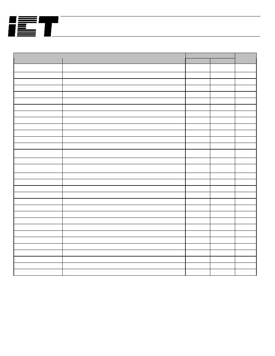
Table 1. Absolute Maximum Ratings
Symbol
Parameter
Conditions
Ratings
Unit
V
CC
Supply Voltage
Relative to Ground
-0.5 to + 7.0
V
V
I
, V
O
Voltage Applied to Any Pin
Relative to Ground
1
-0.5
to
V
CC
+ 0.6
V
I
O
Output Current
Per pin (I
OL
, I
OH
) ±25
mA
T
ST
Storage Temperature
-65 to + 150
∞C
T
LT
Lead Temperature
Soldering 10 seconds
+300
∞C
Table 2. Operating Ranges
Symbol
Parameter
Conditions
Min
Max
Unit
Commercial 4.75
5.2
V
CC
Supply
Voltage
Industrial 4.5
5.5
V
Commercial 0
+70
T
A
Ambient
Temperature
Industrial -40
+85
∞C
T
R
Clock Rise Time
See Note 2
20
ns
T
F
Clock Fall Time
See Note 2
20
ns
T
RVCC
V
CC
Rise Time
See Note 2
250
ms
Table 3. D.C. Electrical Characteristics
Over the Operating Range
Symbol
Parameter
Conditions
Min
Max
Unit
V
OH
Output HIGH Voltage - TTL
V
CC
= Min, I
OH
= -4.0mA
2.4
V
V
OHC
Output HIGH Voltage -
CMOS
V
CC
= Min, I
OH
= -10µA
V
CC
- 0.3
V
V
OL
Output LOW Voltage - TTL
V
CC
= Min, I
OL
= 16mA
0.5
V
V
OLC
Output LOW Voltage -
CMOS
V
CC
= Min, I
OL
= -10µA
0.15
V
V
IH
Input HIGH Level
2.0
V
CC
+ 0.3
V
V
IL
Input
LOW
Level
-0.3
0.8
V
I
IL
Input Leakage Current
V
CC
= Max, GND
'
IN
'
CC
±10
µA
I
OZ
Output Leakage Current
I/O = High-Z, GND
'
O
'
CC
±10
µA
I
SC
Output Short Circuit
Current
4
V
CC
= 5V, V
O
= 0.5V, TA= 25∞C -30
-120
mA
-20
75
I
CC
11
V
CC
Current
V
IN
= 0V or V
CC
3,11
f = 25MHz
All outputs disabled
4
I-20
50 (typ.)
18
85
mA
C
IN
7
Input Capacitance
5
6 pF
C
OUT
7
Output
Capacitance
5
T
A
= 25∞C, V
CC
= 5.0V @ f = 1 MHz
12 pF

7 04-02-050A
Commercial/Industrial
Table 4. A.C Electrical Characteristics Combinatorial
Over the Operating Range
-20/I-20
Symbol
Parameter
6,12
Min
Max
Unit
t
PDI
Propagation delay Internal (t
AL
+ t
LC
)
13
ns
t
PDX
Propagation delay External (t
IA
+ t
AL
+t
LC
+ t
LO
)
20
ns
t
IA
Input or I/O pin to array input
2
ns
t
AL
Array input to LCC
12
ns
t
LC
LCC input to LCC output
10
1
ns
t
LO
LCC output to output pin
5
ns
t
OD
, t
OE
Output Disable, Enable from LCC output
7
5
ns
t
OX
Output Disable, Enable from input pin
7
20
ns
This device has been designed and tested for the recommended operating conditions. Proper operation outside of these
levels is not guaranteed. Exposure to absolute maximum ratings may cause permanent damage
Figure 15. Combinatorial Timing - Waveforms and Block Diagram
8 04-02-050A
Commercial/Industrial
Table 5. A.C. Electrical Characteristics Sequential
-20/I-20
Symbol
Parameter
6,1
Min
Max
Unit
t
SCI
Internal set-up to system clock
8
- LCC
14
(t
AL
+ t
SK
+ t
LC
- t
CK
)
8
ns
t
SCX
Input
16
(EXT.) set-up to system clock, - LCC (t
IA
+ t
SCI
)
10
ns
t
COI
System-clock to Array Int. - LCC/IOC/INC
14
(t
CK
+t
LC
)
7
ns
t
COX
System-clock to Output Ext. - LCC (t
COI
+ t
LO
)
12
ns
t
HX
Input hold time from system clock - LCC
0
ns
t
SK
LCC Input set-up to async. clock
13
- LCC
1
ns
t
AK
Clock at LCC or IOC - LCC output
1
ns
t
HK
LCC input hold time from system clock - LCC
4
ns
t
SI
Input set-up to system clock - IOC/INC
14
(t
SK
- t
CK
)
0
ns
t
HI
Input hold time from system clock - IOC/INC (t
SK
- t
CK
)
5
ns
t
PK
Array input to IOC PCLK clock
9
ns
t
SPI
Input set-up to PCLK clock
17
- IOC/INC (t
SK
-t
PK
-t
IA
)
0
ns
t
HPI
Input hold from PCLK clock
17
- IOC/INC (t
PK
+t
IA
-t
SK
)
10
ns
t
SD
Input set-up to system clock - IOC/INC Sum-D
(
t
IA
+ t
AL
+ t
LC
+ t
SK
- t
CK
)
10
ns
t
HD
Input hold time from system clock - IOC Sum-D
0
ns
t
SDP
Input set-up to PCLK clock - IOC Sum-D
15
(t
IA
+ t
AL
+ t
LC
+ t
SK
- t
PK
)
7
ns
t
HDP
Input hold time from PCLK clock - IOC Sum-D
0
ns
t
CK
System-clock delay to LCC/IOC/INC
6
ns
t
CW
System-clock low or high pulse width
7
ns
f
MAX1
Max. system-clock frequency Int/Int 1/(t
SCI
+ t
COI
)
66.6
MHz
f
MAX2
Max. system-clock frequency Ext/Int 1/(t
SCX
+ t
COI
)
58.8
MHz
f
MAX3
Max. system-clock frequency Int/Ext 1/(t
SCI
+ t
COX
)
50.0
MHz
f
MAX4
Max. system-clock frequency Ext/Ext 1/(t
SCX
+ t
COX
)
45.4
MHz
f
TGL
Max. system-clock toggle frequency 1/(t
CW
+ t
CW
)
9
71.4
MHz
t
PR
LCC presents/reset to LCC output
1
ns
t
ST
Input to Global Cell present/reset (t
IA
+ t
AL
+ t
PR
)
15
ns
t
AW
Asynch. preset/reset pulse width
8
ns
t
RT
Input to LCC Reg-Type (RT)
8
ns
t
RTV
LCC Reg-Type to LCC output register change
1
ns
t
RTC
Input to Global Cell register-type change (t
RT
+ t
RTV
)
9
ns
t
RW
Asynch. Reg-Type pulse width
10
ns
t
RESET
Power-on reset time for registers in clear state
2
5
µs

9 04-02-050A
Commercial/Industrial
Figure 16. Sequential Timing ≠ Waveforms and Block Diagram
Notes
1. Minimum DC input is -0.5V, however inputs may under-shoot to -2.0V
for periods less than 20ns.
2.Test points for Clock and V
CC
in t
R
,t
F
,t
CL
,t
CH
, and t
RESET
are referenced at
10% and 90% levels.
3. I/O pins are 0V or V
CC
.
4. Test one output at a time for a duration of less than 1 sec.
5. Capacitances are tested on a sample basis.
6. Test conditions assume: signal transition times of 5ns or less from the
10% and 90% points, timing reference levels of 1.5V (unless
otherwise specified).
7. t
OE
is measured from input transition to V
REF
±0.1V (See test loads at
end of Section 6 for V
REF
value). t
OD
is measured from input transition
to V
OH
-0.1V or V
OL
+0.1V.
8. DIP: "System-clock" refers to pin 1/21 high speed clocks. PLCC: "Sys-
tem-clock" refers to pin 2/24 high speed clocks.
9. For T or JK registers in toggle (divide by 2) operation only.
10. For combinatorial and async-clock to LCC output delay.
11. ICC for a typical application: This parameter is tested with the device
programmed as a 10-bit D-type counter.
12. Test loads are specified in Section 5 of this Data Book.
13. "Async. Clock" refers to the clock from the Sum term (OR gate).
14. The "LCC" term indicates that the timing parameter is applied to the
LCC register. The "LCC/IOC" term indicates that the timing
parameter is applied to both the LCC and IOC registers. The
"LCC/IOC/INC" term indicates that the timing parameter is applied to
the LCC, IOC, and INC registers.
15. This refers to the Sum-D gate routed to the IOC register for an
additional buried register.
16. The term "input" without any reference to another term refers to an
(external) input pin.
17. The parameter t
SPI
indicates that the PCLK signal to the IOC register
is always slower than the data from the pin or input by the absolute
value of (t
SK
-t
PK
-t
IA
). This means that no set-up time for the data
from the pin or input is required, i.e. the external data and clock can
be sent to the device simultaneously. Additionally, the data from the
pin must remain stable for t
HPI
time, i.e. to wait for the PCLK signal to
arrive at the IOC register.
18. Typical (typ) ICC is measured at T
A
= 25
∞
C, freq = 25MHZ, V
CC
=
5V
10 04-02-050A
Commercial/Industrial
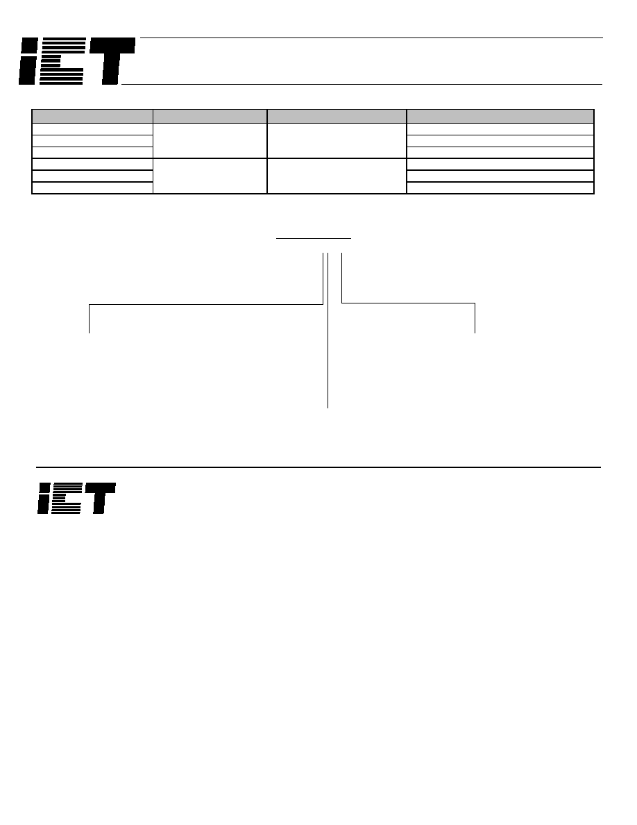
Table 6. Ordering Information
Part Number
Speed
Temperature
Package
PA7572P-20
P40
PA7572F-20
F44
PA7572J-20
13/20ns C
J44
PA7572PI-20
P40
PA7572FI-20
F44
PA7572JI-20
13/20ns
I
J44
Figure 17. Part Number
D evice S uffix
P A 7 5 7 2 J -2 0
P a c k a g e
P = 600m il D IP
F = T hin Q uad F lat P ack (T Q F P )
J = P lastic (J) Leaded C hip C arrier (P LC C )
S p e e d
-20 = 13ns/20ns tpd/tpdx
T e m p e ra tu re R a n g e
(B lank) = C om m ercial 0 to 70∞ C
I = Industrial -40 to +85∞ C
0 8 -1 5 -0 1 7 A
Corporate Office
2123 Ringwood Avenue
San Jose, CA 95131
TEL (408) 434-0678
FAX (408) 432-0815
Email:
sales&marketing@ictpld.com
Website:
http://www.ictpld.com
©2000 Integrated Circuit Technology Corp.
ICT reserves the right to make changes in specifications at any time and without notice. The information furnished by ICT
in this publication is believed to be accurate and reliable. However, no responsibility is assumed by ICT for its use nor for
any infringements of patents or other rights of third parties resulting from its use. No license is granted under any patents
or patent rights of ICT. ICT's products are not authorized for use as critical components in life support devices or systems.
Marks bearing
©
or TM are registered trademarks and trademarks of Integrated Circuit Technology Corp.