1 of 10
General Description
The PEELTM18CV8Z is a Programmable Electrically Erasable
Logic (PEELTM) SPLD (Simple Programmable Logic Device)
that features ultra-low, automatic "zero" power-down operation.
The "zero power" (100 µA max. Icc) power-down mode makes
the PEELTM18CV8Z ideal for a broad range of battery-powered
portable equipment applications, from hand-held meters to PCM-
CIA modems. EE-reprogrammability provides both the conve-
nience of fast reprogramming for product development and quick
product personalization in manufacturing, including Engineering
Change Orders.
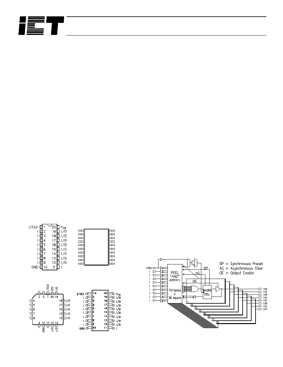
Figure 7 Pin Configuration
PLCC
DIP
SOIC
1
2
3
4
5
6
7
8
9
10
I/CLK
I
I
I
I
I
I
I
I
GND
VCC
I/O
I/O
I/O
I/O
I/O
I/O
I/O
I/O
I
20
19
18
17
16
15
14
13
12
11
TSSOP
The PEELTM18CV8Z is logically and functionally similar to
ICT's 5 Volt PEELTM18CV8 and 3 Volt PEELTM18LV8Z. The
differences between the PEELTM18CV8Z and PEELTM18CV8
include the addition of programmable clock polarity, a product
term clock, and variable width product terms in the AND/OR
Logic Array.
Like the PEELTM18CV8, the PEELTM18CV8Z is logical superset
of the industry standard PAL16V8 SPLD. The PEELTM18CV8Z
provides additional architectural features that allow more logic to
be incorporated into the design. ICT's JEDEC file translator
allows easy conversion of existing 20 pin PLD designs to the
PEELTM18CV8Z architecture without the need for redesign. The
PEELTM18CV8Z architecture allows it to replace over twenty
standard 20-pin DIP, SOIC, TSSOP and PLCC packages.
Figure 8 Block Diagram
CLK MUX (Optional)
TM
Features
s
Ultra Low Power Operation
- Vcc = 5 Volts ±10%
- Icc = 10 µA (typical) at standby
- Icc = 2 mA (typical) at 1 MHz
s
CMOS Electrically Erasable Technology
- Superior factory testing
-
Reprogrammable in plastic package
-
Reduces retrofit and development costs
s
Application Versatility
-
Replaces random logic
-
Super set of standard PLDs
-
Pin-to-pin compatible with 16V8
-
Ideal for use in power-sensitive systems
s
Architectural Flexibility
-
Enhanced architecture fits in more logic
-
113 product terms x 36 input AND array
-
10 inputs and 8 I/O pins
-
12 possible macrocell configurations
-
Asynchronous clear, Synchronous preset
-
Independent output enables
-
Programmable clock; pin 1 or p-term
-
Programmable clock polarity
-
20 Pin DIP/SOIC/TSSOP and PLCC
Commercial
CMOS Programmable Electrically Erasable Logic Device
PEELTM 18CV8Z-25

2 of 10
PEEL
TM
18CV8Z-25
(OPTIONAL)
111
98
83
82
66
49
33
20
21
2
0
10
34
48
65
110
97
I
I
I
I
I/CLK
MACRO
CELL
ASYNCHRONOUS CLEAR
(TO ALL MACROCELLS)
MACRO
CELL
MACRO
CELL
MACRO
CELL
SYNCHRONOUS PRESET
(TO ALL MACROCELLS)
I/O
I/O
I/O
I/O
I/O
I
16
17
15
1
0
3
4
7
8
11
12
15
16
19
20
23
24
27
28
31
32
35
19
112
9
18
2
3
4
MACRO
CELL
I
5
I/O
14
MACRO
CELL
6
MACRO
CELL
I/O
13
7
MACRO
CELL
I/O
12
8
9
11
22
35
50
67
84
I
99
1
11
I
I
Figure 9 PEELTM18CV8Z Logic Array Diagram

3 of 10
PEEL
TM
18CV8Z-25
Function Description
The PEELTM18CV8Z implements logic functions as sum-of-
products expressions in a programmable-AND/fixed-OR logic
array. User-defined functions are created by programming the
connections of input signals into the array. User-configurable
output structures in the form of I/O macrocells further increase
logic flexibility.
Architecture Overview
The PEELTM18CV8Z architecture is illustrated in the block dia-
gram of Figure 8. Ten dedicated inputs and 8 I/Os provide up to
18 inputs and 8 outputs for creation of logic functions. At the
core of the device is a programmable electrically-erasable AND
array that drives a fixed OR array. With this structure, the
PEELTM18CV8Z can implement up to eight sum-of-products
logic expressions.
Associated with each of the eight OR functions is an I/O macro-
cell that can be independently programmed to one of 12 different
configurations. The programmable macrocells allow each I/O to
be used to create sequential or combinatorial logic functions of
active-high or active-low polarity, while providing three different
feedback paths into the AND array.
AND/OR Logic Array
The programmable AND array of the PEELTM18CV8Z (shown in
Figure 9) is formed by input lines intersecting product terms. The
input lines and product terms are used as follows:
s
36 Input Lines:
≠ 20 input lines carry the true and complement of the signals
applied to the 10 input pins
≠ 16 additional lines carry the true and complement values of
feedback or input signals from the 8 I/Os
s
113 product terms:
≠ 102 product terms are used to form sum of product functions
≠ 8 output enable terms (one for each I/O)
≠ 1 global synchronous preset term
≠ 1 global asynchronous clear term
≠ 1 programmable clock term
At each input-line/product-term intersection, there is an
EEPROM memory cell that determines whether or not there is a
logical connection at that intersection. Each product term is
essentially a 36-input AND gate. A product term that is con-
nected to both the true and complement of an input signal will
always be FALSE and thus will not affect the OR function that it
drives. When all the connections on a product term are opened, a
"don't care" state exists and that term will always be TRUE.
When programming the PEELTM18CV8Z, the device program-
mer first performs a bulk erase to remove the previous pattern.
The erase cycle opens every logical connection in the array. The
device is configured to perform the user-defined function by pro-
gramming selected connections in the AND array. (Note that
PEELTM device programmers automatically program all of the
connections on unused product terms so that they will have no
effect on the output function).
Variable Product Term Distribution
The PEELTM18CV8Z provides 113 product terms to drive the
eight OR functions. These product terms are distributed among
the outputs in groups of 8, 10, 12, 14, and 16 to form logical sums
(see Figure 9). This distribution allows optimum use of the
device resources.
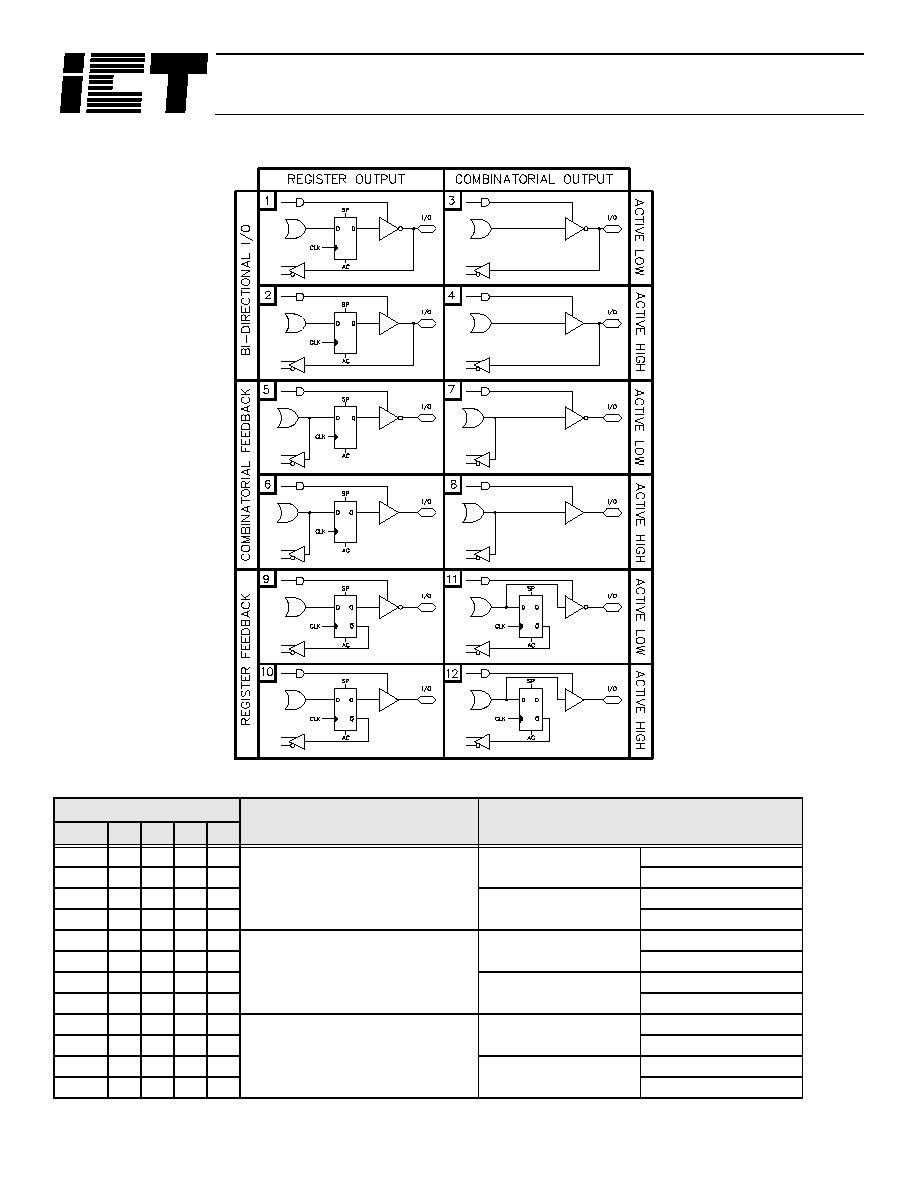
Programmable I/O Macrocell
The unique twelve-configuration output macrocell provides com-
plete control over the architecture of each output. The ability to
configure each output independently lets you to tailor the config-
uration of the PEELTM18CV8Z to the precise requirements of
your design.
Macrocell Architecture
Each I/O macrocell, as shown in Figure 9, consists of a D-type
flip-flop and two signal-select multiplexers. The configuration of
each macrocell is determined by the four EEPROM bits control-
ling these multiplexers. These bits determine output polarity, out-
put type (registered or non-registered) and input-feedback path
(bidirectional I/O, combinatorial feedback). Refer to Table 1 for
details.
Equivalent circuits for the twelve macrocell configurations are
illustrated in Figure 11. In addition to emulating the four PAL-
type output structures (configurations 3, 4, 9, and 10), the macro-
cell provides eight additional configurations. When creating a
PEELTM device design, the desired macrocell configuration is
generally specified explicitly in the design file. When the design
is assembled or compiled, the macrocell configuration bits are
defined in the last lines of the JEDEC programming file.
Output Type
The signal from the OR array can be fed directly to the output pin
(combinatorial function) or latched in the D-type flip-flop (regis-
tered function). The D-type flip-flop latches data on the rising
edge of the clock and is controlled by the global preset and clear
terms. When the synchronous preset term is satisfied, the Q out-
put of the register is set HIGH at the next rising edge of the clock
input. Satisfying the asynchronous clear sets Q LOW, regardless
of the clock state. If both terms are satisfied simultaneously, the
clear will override the preset.
Output Polarity
Each macrocell can be configured to implement active-high or
active-low logic. Programmable polarity eliminates the need for
external inverters.
Output Enable
The output of each I/O macrocell can be enabled or disabled
under the control of its associated programmable output enable
product term. When the logical conditions programmed on the
output enable term are satisfied, the output signal is propagated to

4 of 10
PEEL
TM
18CV8Z-25
the I/O pin. Otherwise, the output buffer is switched into the
high-impedance state.
Under the control of the output enable term, the I/O pin can func-
tion as a dedicated input, a dedicated output, or a bi-directional I/
O. Opening every connection on the output enable term will per-
manently enable the output buffer and yield a dedicated output.
Conversely, if every connection is intact, the enable term will
always be logically false and the I/O will function as a dedicated
input.
Input/Feedback Select
The PEELTM18CV8Z macrocell also provides control over the
feedback path. The input/feedback signal associated with each I/
O macrocell can be obtained from three different locations; from
the I/O input pin, from the Q output of the flip-flop (registered
feedback), or directly from the OR gate (combinatorial feed-
back).
Bi-directional I/O
The input/feedback signal is taken from the I/O pin when using
the pin as a dedicated input or as a bi-directional I/O. (Note that it
is possible to create a registered output function with a bi-direc-
tional I/O, refer to Figure 9).
Combinatorial Feedback
The signal-select multiplexer gives the macrocell the ability to
feedback the output of the OR gate, bypassing the output buffer,
regardless of whether the output function is registered or combi-
natorial. This feature allows the creation of asynchronous latches,
even when the output must be disabled. (Refer to configurations
5, 6, 7, and 8 in Figure 11.)
Figure 9 Block Diagram of the PEELTM18CV8Z
I/O Macrocell
Registered Feedback
Feedback also can be taken from the register, regardless of
whether the output function is programmed to be combinatorial
or registered. When implementing a combinatorial output func-
tion, registered feedback allows for the internal latching of states
without giving up the use of the external output.
Programmable Clock Options
A unique feature of the PEELTM18CV8Z is a programmable
clock multiplexer that allows the user to select true or comple-
ment forms of either input pin or product-term clock sources.
Zero Power Feature
The CMOS PEELTM18CV8Z features "Zero-Power" standby
operation for ultra-low power consumption. With the "Zero-
Power" feature, transition-detection circuitry monitors the inputs,
I/Os (including CLK) and feedbacks. If these signals do not
change for a period of time greater than approximately two t
PD
's,
the outputs are latched in their current state and the device auto-
matically powers down. When the next signal transition is
detected, the device will "wake up" for active operation until the
signals stop switching long enough to trigger the next power-
down. (Note that the tPD is approximately 5 ns. slower on the
first transition from sleep mode.)
As a result of the "Zero-Power" feature, significant power sav-
ings can be realized for combinatorial or sequential operations
when the inputs or clock change at a modest rate. See Figure 5.
Figure 10 Typical ICC vs. Input Clock Frequency
for the 18CV8Z
0.001
0.01
0.1
1
10
100
0.001
0.01
0.1
1
10
ICC in mA.
Frequency in MHz
5 of 10
PEEL
TM
18CV8Z-25
Configuration
Input/Feedback Select
Output Select
#
A
B
C
D
1
0
0
1
0
Bi-directional I/O
Register
Active Low
2
1
0
1
0
Active High
3
0
1
0
0
Combinatorial
Active Low
4
1
1
0
0
Active High
5
0
0
1
1
Combinatorial Feedback
Register
Active Low
6
1
0
1
1
Active High
7
0
1
1
1
Combinatorial
Active Low
8
1
1
1
1
Active High
9
0
0
0
0
Register Feedback
Register
Active Low
10
1
0
0
0
Active High
11
0
1
1
0
Combinatorial
Active Low
12
1
1
1
0
Active High