S2A/A - S2M/A
1.5A SURFACE MOUNT GLASS PASSIVATED RECTIFIER
DS16004 Rev. 7 - 2
1 of 2
S2A/A - S2M/A
Features
@T
A
= 25∞C unless otherwise specified
Notes:
1. Measured at 1.0 MHz and applied reverse voltage of 4.0V DC.
2. Thermal Resistance Junction to Terminal, unit mounted on PC board with 5.0 mm
2
(0.013 mm thick) copper pads as heat sink.
∑
Glass Passivated Die Construction
∑
Low Forward Voltage Drop and High Current
Capability
∑
Surge Overload Rating to 50A Peak
∑
Ideally Suited for Automated Assembly
Single phase, half wave, 60Hz, resistive or inductive load.
For capacitive load, derate current by 20%.
Characteristic
Symbol
S2
A/AA
S2
B/BA
S2
D/DA
S2
G/GA
S2
J/JA
S2
K/KA
S2
M/MA
Unit
Peak Repetitive Reverse Voltage
Working Peak Reverse Voltage
DC Blocking Voltage
V
RRM
V
RWM
V
R
50
100
200
400
600
800
1000
V
RMS Reverse Voltage
V
R(RMS)
35
70
140
280
420
560
700
V
Average Rectified Output Current
@ T
T
= 100∞C
I
(AV)
1.5
A
Non-Repetitive Peak Forward Surge Current 8.3ms
single half sine-wave superimposed on rated load
(JEDEC Method)
I
FSM
50
A
Forward Voltage
@ I
F
= 1.5A
V
FM
1.15
V
Peak Reverse Current
@T
A
= 25∞C
at Rated DC Blocking Voltage @T
A
= 125∞C
I
RM
5.0
125
µA
Typical Total Capacitance (Note 1)
C
T
20
pF
Typical Thermal Resistance, Junction to Terminal
(Note 2)
R
qJT
20
∞C/W
Operating and Storage Temperature Range
T
j,
T
STG
-65 to +150
∞C
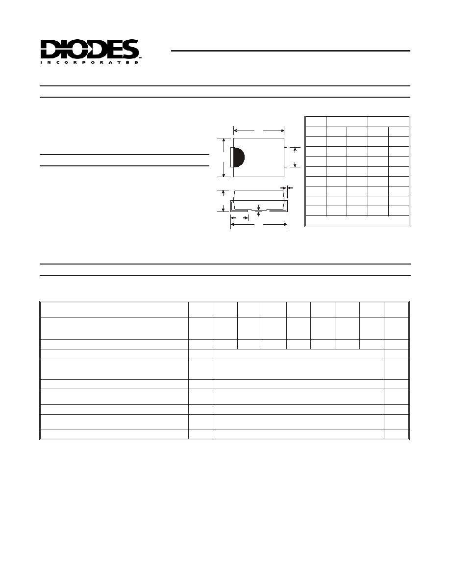
A Suffix Designates SMA Package
No Suffix Designates SMB Package
Mechanical Data
∑
Case: Molded Plastic
∑
Case Material - UL Flammability Rating
Classification 94V-0
∑
Terminals: Solder Plated Terminal -
Solderable per MIL-STD-202, Method 208
∑
Polarity: Cathode Band or Cathode Notch
∑
Approx. Weight: SMA 0.064 grams
SMB 0.093 grams
∑
Marking: Type Number, See Page 2
∑
Ordering Information: See Page 2
SMA
SMB
Dim
Min
Max
Min
Max
A
2.29
2.92
3.30
3.94
B
4.00
4.60
4.06
4.57
C
1.27
1.63
1.96
2.21
D
0.15
0.31
0.15
0.31
E
4.80
5.59
5.00
5.59
G
0.10
0.20
0.10
0.20
H
0.76
1.52
0.76
1.52
J
2.01
2.62
2.00
2.62
All Dimensions in mm
A
B
C
D
G
H
E
J
Maximum Ratings and Electrical Characteristics
SPICE MODELS: S2A S2B S2D S2G S2J S2K S2M
S2AA S2BA S2DA S2GA S2JA S2KA S2MA
XXX = Product type marking code, ex: S2A (SMB package)
XXXX = Product type marking code, ex: S2AA (SMA package)
= Manufacturers' code marking
YWW = Date code marking
Y = Last digit of year ex: 2 for 2002
WW = Week code 01 to 52
YWW
XXX(X)
DS16004 Rev. 7 - 2
2 of 2
S2A/A - S2M/A
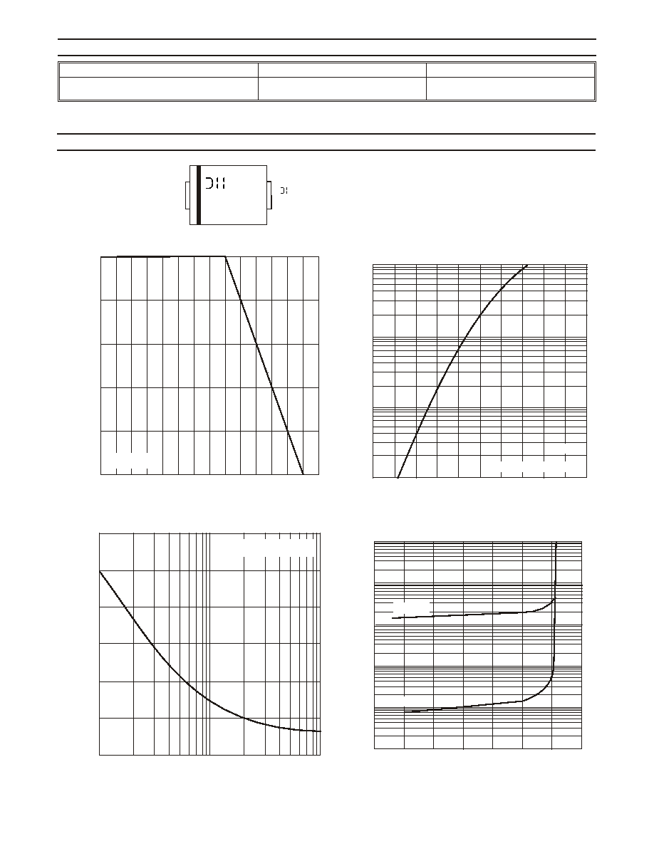
0
0.3
0.6
0.9
1.2
1.5
20
40
60
80
100
120
140
160
T , TERMINAL TEMPERATURE (∫C)
T
Fig. 1 Forward Current Derating Curve
I,
A
V
E
R
A
G
E
F
O
R
W
ARD
C
URRENT
(
A)
AV
Resistive or
inductive load
0.01
0.1
1.0
10
100
1000
0
20
40
60
80
100
120
140
I
,
INST
ANT
A
NE
O
US
REVERSE
CURRENT
(
µA)
R
PERCENT OF RATED PEAK REVERSE VOLTAGE (%)
Fig. 4 Typical Reverse Characteristics
T = 125∞C
j
T = 25∞C
j
0
10
20
30
40
50
60
1
10
100
I
,
PEAK
FOR
W
ARD
SURGE
CURRENT
(A)
FSM
NUMBER OF CYCLES AT 60 Hz
Fig. 3 Forward Surge Current Derating Curve
Single Half-Sine-Wave
JEDEC Method
I
,
INST
ANT
A
NEOUS
FOR
W
ARD
CURRENT
(A)
F
I PULSE WIDTH = 300
mS
F
T = 25∞C
j
0.01
0.1
1.0
10
0.5
0.7
0.9
1.1
1.3
1.5
V , INSTANTANEOUS FORWARD VOLTAGE (V)
F
Fig. 2 Typical Forward Characteristics
Notes:
3. For Packaging Details, go to our website at http://www.diodes.com/datas heets/ap02007.pdf.
* x = Device type, e.g. S2AA-7 (SMA package); S2A-7 (SMB package).
Device*
Packaging
Shipping
S2xA-7
S2x-7
SMA
SMB
5000/Tape & Reel
3000/Tape & Reel
Ordering Information
(Note 3)
Marking Information