DS30298 Rev. 2 - 2
1 of 3
SDM40E20LS
SDM40E20LS
DUAL SURFACE MOUNT SCHOTTKY BARRIER DIODE
Features
Single phase, half wave, 60Hz, resistive or inductive load.
For capacitive load, derate current by 20%.
Maximum Ratings
@ T
A
= 25
∞C unless otherwise specified
Characteristic
Symbol
SDM40E20LS
Unit
Peak Repetitive Reverse Voltage
Working Peak Reverse Voltage
DC Blocking Voltage
V
RRM
V
RWM
V
R
20
V
RMS Reverse Voltage
V
R(RMS)
14
V
Forward Continuous Current (Note 1)
I
FM
0.4
A
Non-Repetitive Peak Forward Surge Current
8.3ms single half sine-wave superimposed on rated load
(JEDEC Method)
I
FSM
2
A
Power Dissipation (Note 1)
P
d
225
mW
Typical Thermal Resistance Junction to Ambient (Note 1)
R
qJA
444
∞C/W
Power Dissipation (Note 2)
P
d
300
mW
Typical Thermal Resistance Junction to Ambient (Note 2)
R
qJA
333
∞C/W
Operating and Storage Temperature Range
T
j,
T
STG
-55 to +125
∞C
A
E
J
L
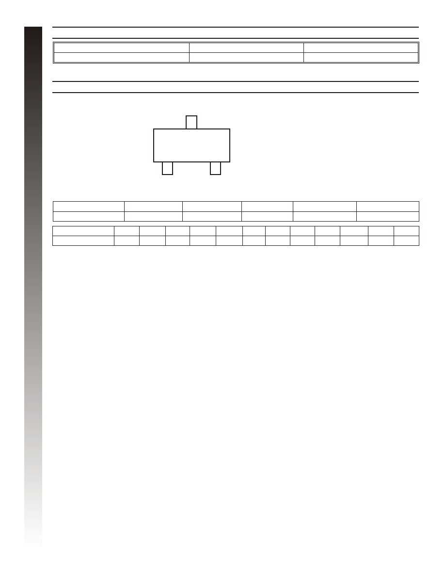
TOP VIEW
M
B
C
H
G
D
K
∑
Very Low Forward Voltage Drop
∑
Guard Ring Construction for
Transient Protection
∑
High Conductance
∑
Case: SOT-23, Plastic
∑
Case material - UL Flammability Rating
Classification 94V-0
∑
Moisture sensitivity: Level 1 per J-STD-020A
∑
Polarity: See Diagram
∑
Leads: Solderable per MIL-STD-202,
Method 208
∑
Marking: Date Code and Type Code
∑
Type Code: KSW
Weight: 0.004 grams (approx.)
∑
Ordering Information: See Page 3
Mechanical Data
Electrical Characteristics
@ T
A
= 25
∞C unless otherwise specified
Characteristic
Symbol
Min
Typ
Max
Unit
Test Conditions
Reverse Breakdown Voltage (Note 3)
V
(BR)R
20
æ
æ
V
I
R
= 0.5mA
Forward Voltage Drop (Note 3)
V
F
æ
æ
æ
æ
0.310
0.430
V
I
F
= 0.1A
I
F
= 0.5A
Leakage Current (Note 3)
I
R
æ
æ
æ
æ
100
250
mA
V
R
= 10V
V
R
= 20V
Total Capacitance
C
T
æ
170
æ
pF
f = 1MHz, V
r
= 0VDC
T
C
U
D
O
R
P
W
E
N
Notes:
1. Device mounted on FR-5 1.0 x 0.75 x 0.062 inch PCB pad layout as shown on Diodes Inc. suggested pad layout AP02001,
which can be found on our website at http://www.diodes.com/datasheets/ap02001.pdf.
2. Device mounted on Alumina PCB, 0.4 inch x 0.3 inch x 0.024 inch; pad layout as shown on Diodes Inc. suggested pad layout
document AP02001, which can be found on our website at http://www.diodes.com/datasheets/ap02001.pdf.
3. Short duration test pulse used to minimize self-heating effect.
SOT-23
Dim
Min
Max
A
0.37
0.51
B
1.20
1.40
C
2.30
2.50
D
0.89
1.03
E
0.45
0.60
G
1.78
2.05
H
2.80
3.00
J
0.013
0.10
K
0.903
1.10
L
0.45
0.61
M
0.85
0.80
a
0
∞
8
∞
All Dimensions in mm

DS30298 Rev. 2 - 2
2 of 3
SDM40E20LS
T
C
U
D
O
R
P
W
E
N
0
0.10
0.20
0
50
100
150
I
,
A
VERAGE
F
O
R
W
ARD
CURRENT
(A)
F(A
V
)
T , TERMINAL TEMPERATURE (
∞C)
T
Fig. 1 Forward Current Derating Curve
0.30
0.40
25
75
125
0.01
0.1
1.0
10
0.2
0
0.4
0.6
0.8
1.0
I
,
INST
ANT
A
NEOUS
FWD
CURRENT
(A)
F
V , INSTANTANEOUS FORWARD VOLTAGE (V)
F
Fig. 2 Typical Forward Characteristics
T = 25
∞C
j
10
100
1000
0
5
10
15
20
25
V , REVERSE VOLTAGE (V)
R
Fig. 3 Typical Reverse Characteristics
T = 25
∞C
j
C
,
CAP
A
CIT
ANCE
(
pF)
T
V , REVERSE VOLTAGE (V)
R
Fig. 4 Typ. Total Capacitance vs Reverse Voltage
1000
1.0
10
100
0
5
10
15
20