DIONICS, INC.
Phone: (516) 997-7474
65 Rushmore Street
Fax: (516) 997-7479
Westbury, NY 11590
Website: www.dionics-usa.com
LEVEL-SHIFTED VACUUM FLUORESCENT DISPLAY DRIVERS
DI-512BR*
DI-513BR
DI-514BR
(* Also directly applicable as gas discharge display digit driver. Pin for pin replacement for SPRAGUE UDN6184A)
General Description:
The DIONICS DI-512BR, DI-513BR and DI-514BR circuits are designed for interfacing between MOS or TTL
logic circuitry and vacuum fluorescent display panels. Each section of these devices consists of a switched
constant current level shifter (capable of 50 Volt, 80 Volt or 110 Volt operation) and a PNP-NPN driver
transistor pair. The constant current operation of the level shifter stage results in low power dissipation. Input
circuitry is suitable for open drain PMOS, CMOS, open-collector or standard TTL.
Features:
¸
50V, 80V and 110VLevel Shift Capability
¸
MOS and TTL Compatibility
¸
Segment and Digit Drivers
¸
Low Power Dissipation
¸
Reliable Silicon Dielectrically IC Process
¸
Pin for Pin replacement for SPRAGUE UDN6118A, UDN6128A
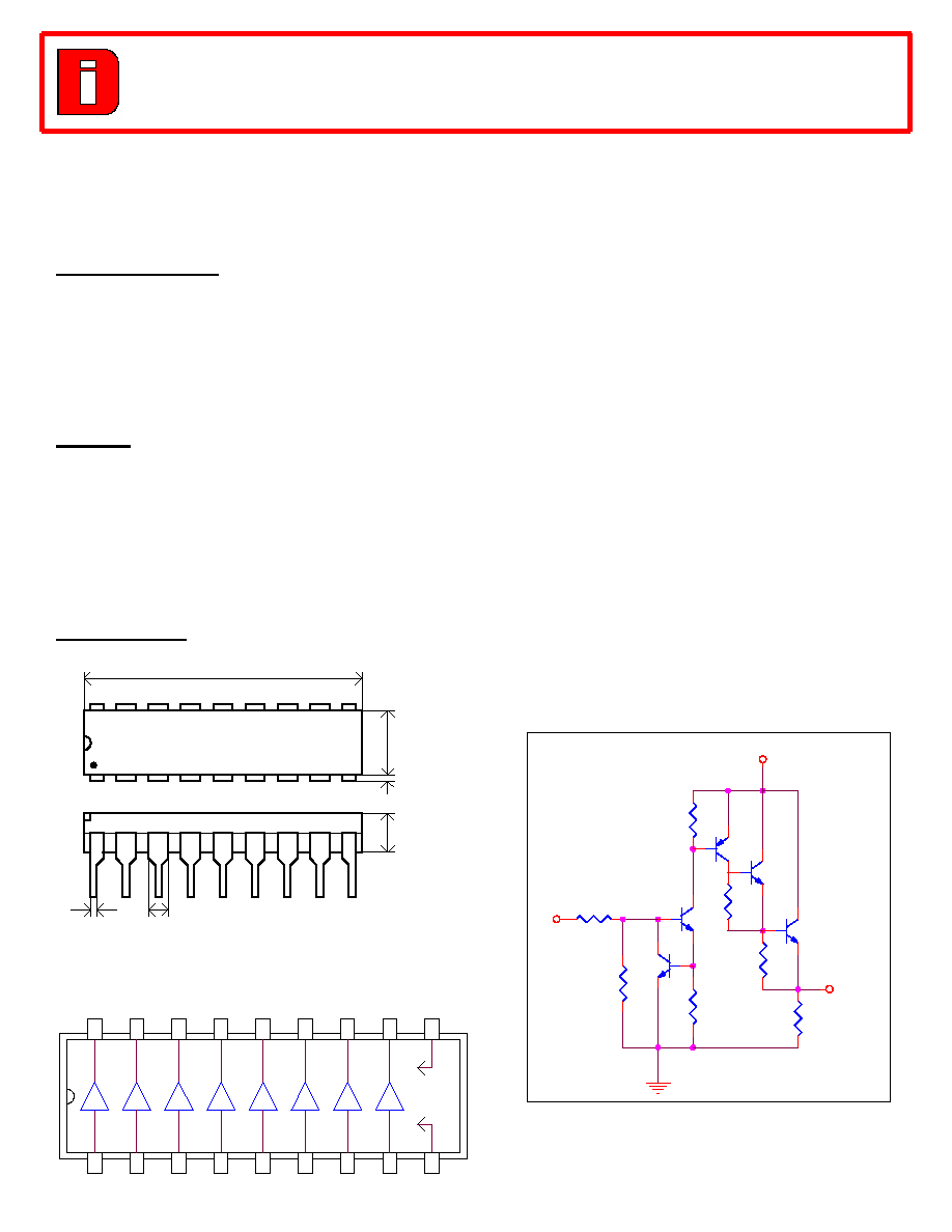
Package Layout:
0.025
0.900
0.020
0.185
0.250
DIONICS INC
DI-514BR
0.070
15
GND
11
1
In
In
Out
18
Out
6
7
17
Out
8
16
5
2
10
13
In
In
4
Out
V +
Out
In
Out
12
14
In
In
Out
3
In
Out
DI-512BR DI-513BR DI-514BR
9
Circuit Schematic
(Each Section)
Input
Rpd
V+
Output
03/2002

Absolute Maximum Ratings (T
A
= 25
0
C)
Characteristic
Symbol
Note
Limit
Unit
DI-514BR DI-513BR DI-512BR
Supply Voltage
V
CC
Measured with respect to GND terminal
50
80
110
V
Input Voltage
V
I
Measured with respect to GND terminal
30
30
30
V
Output Voltage
V
O
Measured with respect to V+ terminal
50
80
110
V
Output Current
I
O
30
30
30
mA
Power Dissipation
P
D
Derate at 8mW/
0
C, above 25
0
C ambient
800
800
800
mW
Storage Temperature
T
S
-55
0
C
To
+125
0
C
0
C
Operating Temperature
T
O
0
0
C
To
+70
0
C
0
C
Electrical Characteristics (T
A
= 25
0
C)
Parameter
Symbol
Note
Condition
Typ. Max. Unit
Output Saturation Voltage
V
OS (ON)
Measured with
respect to V+
terminal
I
O
=20mA;
V
I
=2.4V;
V
CC
= 40V
3
5
V
Supply Leakage
I
CC (OFF)
Derate at 8mW /
0
C;
above 25
0
C ambient
v
DI-514BR
V
I
= 0.4V;
V
CC
= 50V
10
15
µ
A
v
DI-513BR
V
I
= 0.4V;
V
CC
= 80V
10
15
µ
A
v
DI-512BR
V
I
= 0.4V;
V
CC
= 110V
10
15
µ
A
Input Current
I
O (ON)
V
I
=2.4V
300
400
µ
A
Supply Current
I
CC
One Input at 2.4V,
Other at 0.4V
I
O
= 0mA;
V
I
= 0.4V;
V
CC
= 50V 0.5
1.0
mA
Min. Max. Unit
Pull down Current
I
PD
I
O
= 0mA;
V
I
= 0.4V;
V
O
= 40V 200
500
µ
A
Pull down Resistors
R
PD
80
200
k
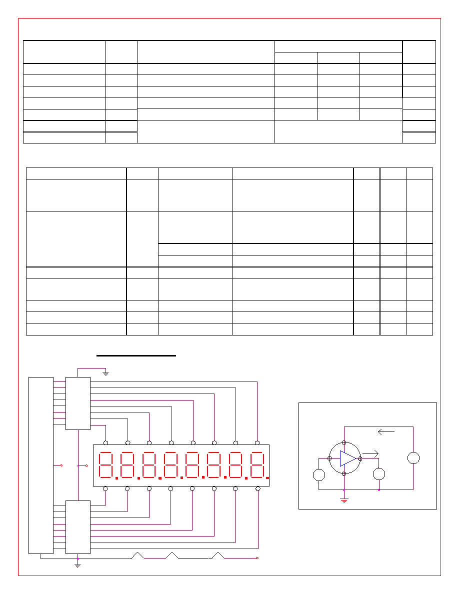
Typical Application:
D
B
D8
DISPLAY CONTROL LOGIC
4
A
+35V
9
7
13
10
C
8
14
B
6
17
A
5
10
+5V
18
8
2
16
DIONICS INC.
DI-514BR
3
7
1
15
8
6
9
12
7
5
VFIL
16
11
D6
5
4
DEC
15
13
D5
3
G
14
D2
2
DEC
F
6
17
D1
12
G
E
1
18
D3
11
F
D
2
DIONICS INC.
DI-514BR
3
D4
E
C
4
D7
1
Simplified Test Circuit
Vo
V +
Io
Vi
Icc
+
-
-
+
Vcc
GND
+
-

