DIONICS, INC.
65 Rushmore Street
Westbury, NY 11590
Phone: (516) 997-7474
Fax: (516) 997-7479
Website: www.dionics-usa.com
OPTO-ISOLATED PHOTOVOLTAIC ISO-GATE
TM
MOSFET DRIVERS
DIG-11-06-030
DIG-11-06-150
DIG-11-08-050
DIG-12-06-025
DIG-12-08-010
DIG-12-08-045
DIG-12-06-100
DIG-12-06-250
Features:
�
Completely Isolated Voltage Signal Generation
�
Dielectrically Isolated
�
Logic Circuit Compatibility
�
High Open Circuit Voltage
�
High Operating Temperature
�
Fast Response Time
�
High Isolation Resistance
�
Excellent Input/Output Linearity
�
Self Limiting Gate Voltage
Applications:
�
Gate Drive For MOS devices
�
Gate Drive For SCR
�
Solid-State Relays
�
Interface Between Logic Circuits & External Loads
�
A.T.E. (Automatic Test Equipment)
�
Switching Equipment
�
Isolation Amplifiers
�
Load Control From Microprocessor I/O Ports
�
Thermocouple Open Detectors
Description:
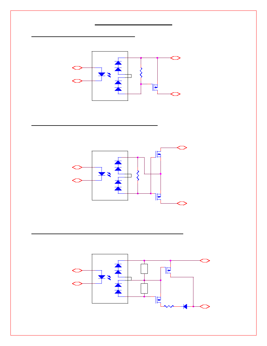
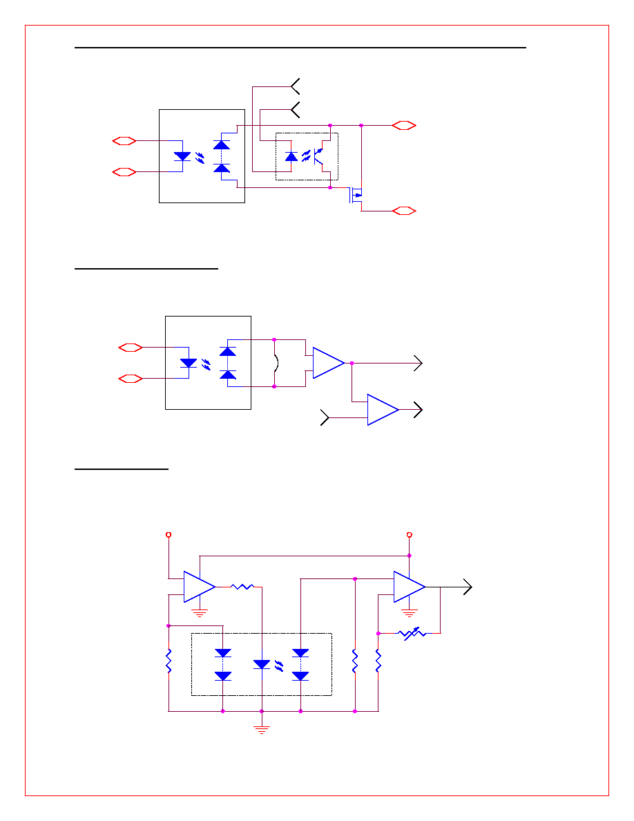
The photovoltaic MOSFET driver is a State-of- the-Art, optically coupled floating power source used primarily to control
MOSFETs when electrical isolation between input and output is required. The ISO-GATE
TM
is a state-of-the-art opto-
isolator incorporating DIONICS' photovoltaic (PV) diode arrays and an infrared LED. The diode array is a unique I.C.
consisting of series-connected photovoltaic diodes. The diodes are completely isolated from each other and from their
common substrate by means of SiO
2
Dielectric Isolation (DI). These photovoltaic output chips are electrically isolated but
optically coupled to the LED.
The typical input circuit to the LED is a limiting resistor connected in series with the LED. When activated, the LED
emits infrared light towards the photovoltaic diode array, which then responds by generating an open circuit voltage
(Voc). This Voc is floating and is therefore completely isolated. The Voc value depends on the LED input drive and load
impedance. DIONICS, Inc offers a wide variety of package styles including low-cost plastic Mini-DIP's, high reliability
TO-5 metal cans, 8-pin ceramic side brazed DIP's and ceramic chip carriers for hybrid manufacturers. Other custom
packages and custom designs are also available.
o
Group I: DIG-11-06-030; DIG-11-06-150; DIG-11-08-050.
o
Group II: DIG-12-06-025; DIG-12-06-100; DIG-12-06-250; DIG-12-08-010; DIG-12-08-045.
v
Package Layout:
0.025
0.185
0.250
DIG-11
06-030
xxxx
0.070
0.380
0.020
0.020
0.185
0.250
0.025
DIG-12
08-045
xxxx
0.070
0.380
11/2001
v
Pin Designation
Pin Number
Group I
Group II
1
Input +
Input +
2
Input -
Input -
3
Not Connected Not Connected
4
Not Connected Not Connected
5
Not Connected
Output1+
6
Output +
Output1-
7
Not Connected
Output2+
8
Output -
Output2-
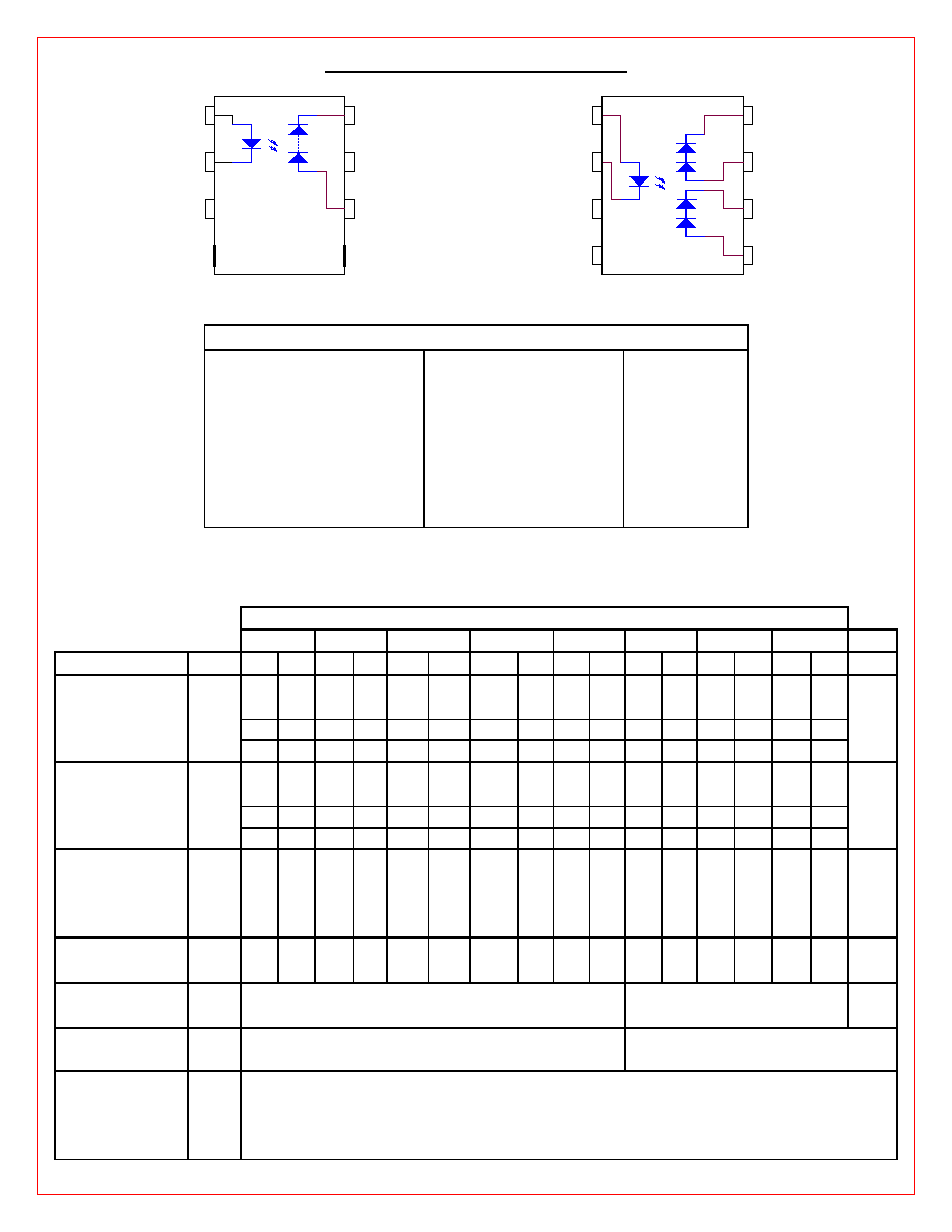
Group I and Group II Equivalent Circuits:
8
3
2
1
7
6
LED
PV
2
1
PV
8
5
LED
PV
4
7
6
3
Group I
Group II
* Note: DIG-12-06-100 and DIG-12-06-250 are rated @ 3.4 V Max.
v
Individual Channel Electrical Characteristics (T
a
=25
0
C)
MODEL NUMBERS DIG -
12-08-010 12-06-025 12-08-045 12-06-100 12-06-250 11-06-030 11-08-050 11-06-150 Unit
Parameter
Symbol Min. Typ. Min. Typ. Min. Typ. Min. Typ. Min. Typ. Min. Typ. Min. Typ. Min. Typ.
Open Circuit Voltage
V
oc
I
led
= 2mA
6.0
8.0
5.0 6.5
7.0
8.0
5.0
6.0 5.0 6.0 4.5 5.5 6.5
9.0
5.0
6.0
V
I
led
= 10mA
8.0
9.0
6.5 7.5
8.5
9.0
6.5
7.0 6.5 7.3 6.0 6.5 7.5 10.0 6.5
7.0
V
I
led
= 30mA
9.0 10.0 7.0 6.3
9.5
10.0
7.5
7.8 7.5 8.0 6.5 7.0 8.5 11.0 7.5
8.0
V
Short Circuit Current
I
sc
I
led
= 2mA
0.2
0.5
0.5 1.0
0.6
1.0
1.0
2.0 2.0 3.0 0.15 1.1 0.6
2.0
1.5
3.0
�
�
A
I
led
= 10mA
1.35 3.0
3.0 6.0
4.0
8.0
8.0
12.0 12.5 25.0 1.0 7.0 4.0 13.0 10.0 18.0
�
�
A
I
led
= 30mA
4.0
9.0
9.0 20.0 12.0 25.0
30.0 40.0 37.5 75.0 3.5 20.0 12.0 40.0 30.0 55.0
�
�
A
Turn-On Time
I
f
= 50 mA; C = 10pF
P.W = 100us;
T
on
-
3.0
- 10.0
-
8.0
-
3.0
-
3.0
-
8.0
-
5.0
-
3.0
�
�
s
f =1kHz; R
s
= 10M
Temp. Coefficient
-
-100
-
-80
-
-100
-
-80
-
-80
-
-40
-
-50
-
-40
mV/
0
C
(Channels in Series)
Isolation Voltage
V
iso
I
iso
= 50
�
A @ 2 sec
2500
2500
VDC
Operating Temp.
T
op
-50
0
C To
+100
0
C
-50
0
C To +80
0
C
(Channels in Series)
Turn-Off Time
T
off
I
f
= 50 mA; C = 10pF
The Photovoltaic array stops generating current within one microsecond of the trailing edge
P.W = 100us;
of LED current the discharge time is solely dependent upon discharge circuitry and capacitive load.
f =1kHz; R
s
= 10M
v
Absolute Maximum Ratings (T
a
= 25
0
C)
LED Forward Current
LED Forward Current
LED Forward Voltage
LED Reverse Current
LED Reverse Voltage
Output Forward Voltage
Lead Soldering Time
Storage Temperature
Power Dissipation
Steady State
Peak 10% Duty Cycle
I
f
= 20mA
V
r
= 3V
I
f
= 10�A
At 260
0
C
100 mA
250 mA
1.7V*
100�A
5V
20V
10 sec
-50 to 125
0
C
150 mW