DIONICS, INC.
65 Rushmore Street
Westbury, NY 11590
Phone: (516) 997-7474
Fax: (516) 997-7479
Website: www.dionics-usa.com
DI-8884A High Voltage Cathode Decoder/Driver
Direct Replacement for National DM-8884A
General Description:
The DI-8884A is designed to decode four
lines of BCD input and drive seven segment
digits of gas-filled readout displays. Two
separate inputs are provided for driving the
decimal point and comma cathodes.
All outputs consist of switchable and
programmable current sinks, which provide
constant current to the tube cathodes, even
with high tube anode supply tolerance.
Output currents may be varied over the 0.2
to 1.2 mA range for multiplex operation.
The output current is adjusted by connecting
an external program resistor (R
p
) from V
cc
to
the program input.
Features:
� Reliable Dielectric Isolation Process
� Current Sink Outputs
� High Output Breakdown Voltage
� Low Input Load Current
� Intended For Multiplex Operation
� Replacement For National DM-8884A
� Standard 18-pin DIP Package
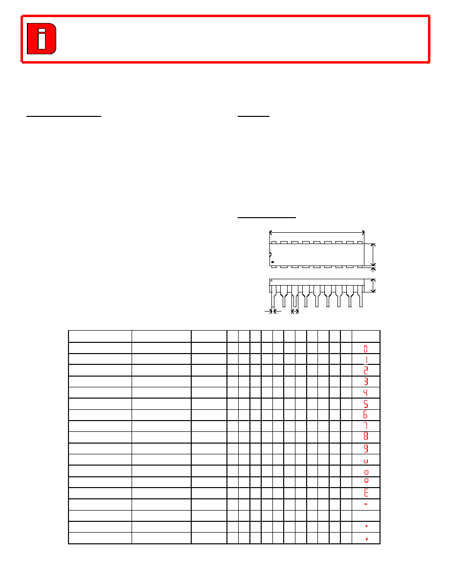
Package Layout:
v
Truth Table
Function
Decimal Point Comma
D C B A a b c d e f g
Display
0
1
1
0 0 0 0 0 0 0 0 0 0 1
1
1
1
0 0 0 1 1 0 0 1 1 1 1
2
1
1
0 0 1 0 0 0 1 0 0 1 0
3
1
1
0 0 1 1 0 0 0 0 1 1 0
4
1
1
0 1 0 0 1 0 0 1 1 0 0
5
1
1
0 1 0 1 0 1 0 0 1 0 0
6
1
1
0 1 1 0 0 1 0 0 0 0 0
7
1
1
0 1 1 1 0 0 0 1 1 1 1
8
1
1
1 0 0 0 0 0 0 0 0 0 0
9
1
1
1 0 0 1 0 0 0 0 1 0 0
10
1
1
1 0 1 0 1 1 0 0 0 1 1
11
1
1
1 0 1 1 1 1 0 0 0 1 0
12
1
1
1 1 0 0 0 0 1 1 1 0 0
13
1
1
1 1 0 1 0 1 1 0 0 0 0
14
1
1
1 1 1 0 1 1 1 1 1 1 0
15
1
1
1 1 1 1 1 1 1 1 1 1 1
*Decimal Point
0
1
X X X X X X X X X X X
*Comma
0
0
X X X X X X X X X X X
*Decimal point and Comma can be displayed with or without any numeral.
09/2001
0.900
DIONICS
DI-8884A
0.070
0.250
0.020
0.025
0.185

DI-8884A High Voltage Cathode Decoder/Driver
v
Electrical Characteristics ( 0
0
C < T
a
< 70
0
C - Unless otherwise noted; Vcc = 5V � 5% )
Parameter
Conditions
Min. Max. Unit
Logic "1" Input Voltage
V
cc
= 4.75V
2.0
-
V
Logic "0" Input Voltage
V
cc
= 4.75V
-
1.0 V
Logic "1" Input Current
V
cc
= 5.25V; V
in
= 2.4V
-
15.0 �A
Logic "0" Input Current
V
cc
= 5.25V; V
in
= 0.4V
-
-250 �A
Positive Input Clamp Voltage
V
cc
= 4.75V; I
in
= 1.0mA
5.0
-
V
Negative Input Clamp Voltage V
cc
= 5.0 V; I
in
= -12.0 mA; @T
a
= 25
0
C
-
-1.5 V
Power Supply Current
V
cc
= 5.25V; R
p
= 2.8K; All V
in
= 5V
-
40.0 mA
Segment Outputs
All Outputs On Current Ration
All V
out
= 50V
Output b Current = Ref.
0.9 1.1
-
Output b On Current
V
cc
= 5V; V
out
@ b=50V; @T
a
= 25
0
C
R
p
= 18.1K
0.18 0.22 mA
R
p
= 7.03K
0.45 0.55 mA
R
p
= 3.40 K
0.90 1.10 mA
R
p
= 2.80K
1.08 1.32 mA
Output Leakage Current
V
out
= 75V
-
5.0 �A
Output Breakdown Voltage
I
out
= 10�A
110
-
V
Propagation Delay
Any Input to Segment Output
V
cc
= 5V; @T
a
= 25
0
C
-
10.0 � s
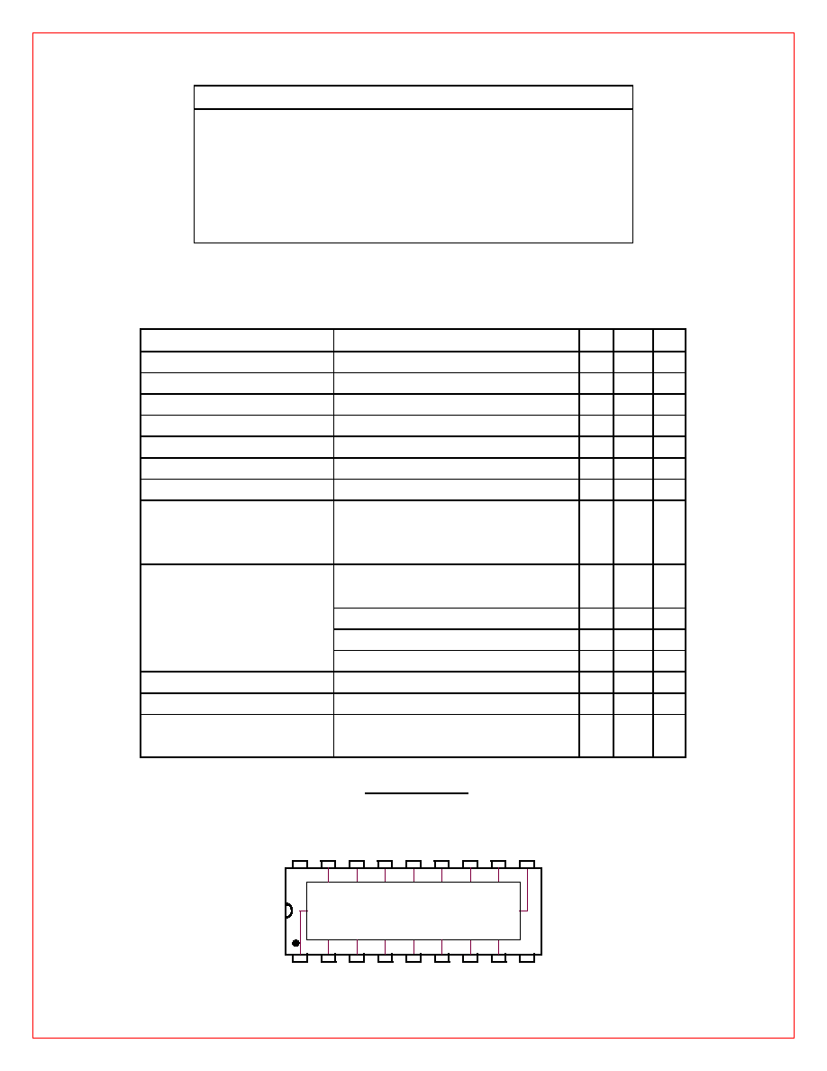
v Pin Designation
D
A
17
Vcc
Prog.
Input
15
7
GND
8
6
12
COM
OUT
5
c
16
b
f
DP
IN
a
3
9
10
d
4
18
2
g
13
1
11
e
B
C
14
DP
OUT
COM
IN
v Absolute Maximum Ratings
Input Voltage (Vcc)
7V
Segment Output Voltage
110V
Power Dissipation
600mW
Transient Segment Output Current
50mA
Operation Temperature Range
0
0
C to 70
0
C
Storage Temperature Range
-65
0
C to 150
0
C

