
DESCRIPTION:
The DP5Z1MW32PV3 `'VERSA-STACK'' module is a memory subsystem
using DPAC Technologies' ceramic Stackable Leadless Chip Carriers
(SLCC) mounted on a co-fired ceramic substrate. It offers 32 Megabits of
FLASH EEPROM in a single package envelope of 1.090" x 1.090" x .163".
The DP5Z1MW32PV3 is built with 2 SLCC packages each containing
1Meg x 16 FLASH memory devices. Each SLCC is hermetically sealed,
making the module suitable for commercial, industrial and military
applications.
By using SLCCs, the `'Versa-Stack'' family of modules offers a higher
board density of memory than available with conventional through-hole,
surface mount, module or hybrid techniques.
FEATURES:
∑
Organizations Available:
1 Meg x 32, 2 Meg x 16
∑
Fast Access Times:
120, 150, 200ns (max.)
∑
Single 5.0 Volt
∑
High-Density Symmetrically Blocked Architecture
- Sixteen 128 Kbyte Blocks Per Device
∑
Extended Cycling Capability
- 100K Write/Erase Cycles
∑
Automated Erase and Program Cycles
- Command User Interface
- Status Register
∑
SRAM-Compatible Write Interface
∑
Hardware Data Protection Feature
- Erase / Write Lockout during
Power Transitions
∑
66 - Pin PGA `'VERSA-STACK'' Package
30A180-11
1
Rev. D 5/02
This document contains information on a product that is currently released to production at DPAC Technologies Corp.
DPAC reserves the right to change products or specifications herein without prior notice.
PIN-OUT DIAGRAM
FUNCTIONAL BLOCK DIAGRAM
PIN NAMES
A0 - A19
Address Inputs
I/O0 - I/O31
Data Input/Output
CE0, CE1
Chip Enables
WE
Write Enables
OE
Output Enables
V
DD
Power (+5 Volts)
V
SS
Ground
N.C.
No Connect
32 Megabit FLASH EEPROM
DP5Z1MW32PV3
30A180-11
www.dpactech.com
2
Rev. D 5/02
32 Megabit FLASH EEPROM
DP5Z1MW32PV3
PIN NAMES
A0 - A19
ADDRESS INPUTS: for memory address. Addresses are internally latched during a write cycle.
I/O0 - I/O31
DATA INPUT/OUTPUT: Input data commands during Command Interface Register (CIR) write cycles.
Output array, status and identifier data in the appropriate read mode. Floats when the chip is de-selected
or the outputs are disabled.
CE0, CE1
CHIP ENABLES: Activate the device's control logic, input buffers, decoders and sense amplifiers. With CE high, the
device is de-selected and per consumption reduces to Standby level upon completion of any current program or erase
operation. CE must be low to select the device. Device selection occurs with the falling edge of CE. The rising edge of
CE disables the device.
WE
WRITE ENABLES: Controls writes to the Command Interface Register (CIR). WE is active low.
OE
OUTPUT ENABLES: Gates the device's data through the output buffers during a read cycle. OE is active low.
V
DD
DEVICE POWER SUPPLY: (+5 Volts
±
10%)
V
SS
GROUND
N.C.
NO CONNECT
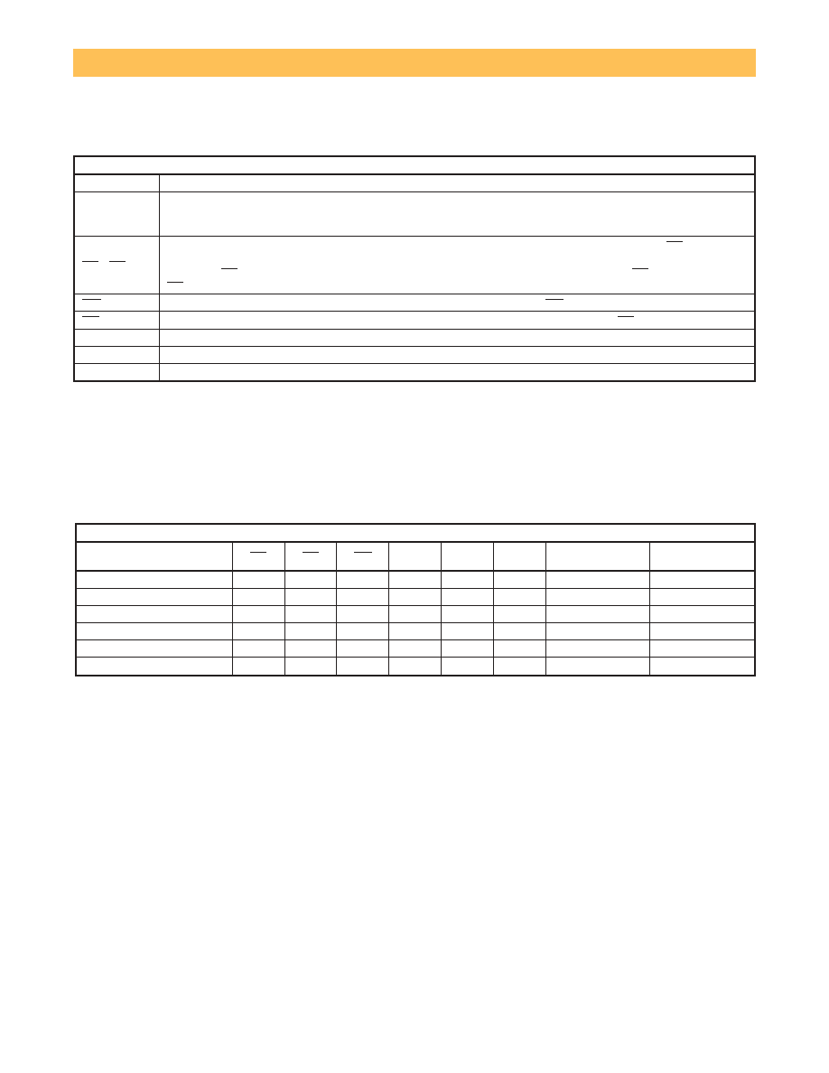
BUS OPERATION
11
Flash memory reads, erases and writes in-system via the local CPU. All bus cycles to or from the flash memory conform to standard
microprocessor bus cycles.
Table 1: Bus Operation
Mode
CE
OE
WE
A0
A1
A9
I/O0 - I/O7
(I/O16 - I/O23)
I/O8 - I/O15
(I/O24 - I/O31)
Read
1, 4
V
IL
V
IL
V
IH
X
X
X
D
OUT
HIGH-Z
Output Disable
1
V
IL
V
IH
V
IH
X
X
X
HIGH-Z
HIGH-Z
Standby
1
V
IH
X
X
X
X
X
HIGH-Z
HIGH-Z
Manufacturer Identifier
1, 3
V
IL
V
IL
V
IH
V
IL
V
IL
V
ID
C2H
00H
Device Identifier
3
V
IL
V
IL
V
IH
V
IH
V
IL
V
ID
FAH/F1H
12
00H
Write
1, 2
V
IL
V
IH
V
IL
X
X
X
D
IN
D
IN
NOTES:
a.
X can be V
IL
or V
IH
for address or control pins.
b.
Command for different Erase operations, Data program operations can only be successfully completed through proper command sequence.
c.
V
ID
= 11.5V - 12.5V.
WRITE OPERATION
Commands are written to the COMMAND INTERFACE REGISTER
(CIR) using standard microprocessor write timing. The CIR serves
as the interface between the microprocessor and the internal chip
operation. The CIR can decipher Read Array, Read Silicon ID,
Erase and Program command. In the event of a read command,
the CIR simply points the read path at either the array or the Silicon
ID, depending on the specific read command given. for a program
or erase cycle, the CIR informs the write state machine that a
program or erase has been requested. During a program cycle, the
write state machine control the program sequences and the CIR will
only respond to status reads. During a sector/chip erase cycle, the
CIR will respond to status reads and erase suspend. After the write
state machine has completed its task, it will allow the CIR to
respond to its full command set. The CIR stays at read status
register mode until the microprocessor issues another valid
command sequence.
Device operations are selected by writing commands into the CIR.
Table 3 below defines 16 Megabit Flash family command.

30A180-11
www.dpactech.com
3
Rev. D 5/02
32 Megabit FLASH EEPROM
DP5Z1MW32PV3
DEVICE OPERATION
SILICON ID READ
The Silicon ID Read mode allows the reading out of a binary code
from the device and will identify its manufacturer and type. this is
intended for use by programming equipment for the purpose of
automatically matching the device to be programmed with its
corresponding programming algorithm. This mode is functional
over the entire temperature range of the device.
To activate the mode, the programming equipment must force V
ID
(11.5V ~ 12.5V) on address pin A9. Two identifier bytes may then
be sequenced from the device outputs by toggling address A0 from
V
IL
to V
IH
. All addresses are don't cares except A0 and A1.
The manufacturer and device codes may also be read via the
command register, for instance when the device is erased or
programmed in a system without access to high voltage on the A9
pin. The command sequence is illustrated in Table 2.
To terminate the operation, it is necessary to write the read/reset
command sequence into the CIR.
READ RESET COMMAND
The read or reset operation is initiated by writing the read/reset
command sequence into the command register. Microprocessor
read cycles retrieve array data from the memory. The device
remains enabled for reads until the CIR contents are altered by a
valid command sequence.
The device will automatically power-up in the read/reset state. In
this case, a command sequence is not required to read data. This
default value ensures that no spurious alteration of the memory
content occurs during the power transition. Refer to the AC Read
Characteristics and Waveforms for the specific timing parameters.
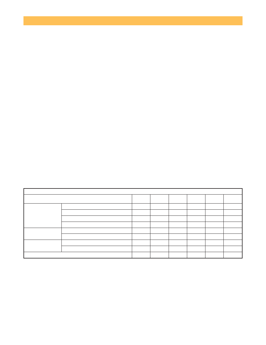
Table 2: Command Definition
11
Command
Sequence
Bus
Cycles
Req'd
First Bus
Write Cycle
Second Bus
Write Cycle
Third Bus
Write Cycle
Fourth Bus
Read/Write Cycle
Fifth Bus
Write Cycle
Sixth Bus
Write Cycle
Address
Date
Address
Date
Address
Date
Address
Date
Address
Data
Address
Data
Read/Reset
4
5555H
AAH
2AAAH
55H
5555H
F0H
RA
RD
-
-
-
-
Silicon ID Read
4
5555H
AAH
2AAAH
55H
5555H
90H
00H/01H
C2H/FIH
-
-
-
-
Page/Byte Program
4
5555H
AAH
2AAAH
55H
5555H
A0H
PA
PD
-
-
-
-
Chip Erase
6
5555H
AAH
2AAAH
55H
5555H
80H
5555H
AAH
2AAAH
55H
5555H
10H
Sector Erase
6
5555H
AAH
2AAAH
55H
5555H
80H
5555H
AAH
2AAAH
55H
SA
30H
Erase Suspend
3
5555H
AAH
2AAAH
55H
5555H
B0H
-
-
-
-
-
-
Erase Resume
3
5555H
AAH
2AAAH
55H
5555H
D0H
-
-
-
-
-
-
Read Status
Register
4
5555H
AAH
2AAAH
55H
5555H
70H
X
SRD
-
-
-
-
Clear Status
Register
3
5555H
AAH
2AAAH
55H
5555H
50H
-
-
-
-
-
-
Sleep
3
5555H
AAH
2AAAH
55H
5555H
C0H
-
-
-
-
-
-
Abort
3
5555H
AAH
2AAAH
55H
5555H
E0H
-
-
-
-
-
-
NOTES:
Address bit A15 - A19 = X = Don't Care for all address commands except for Programming Address (PA) and Sector Address (SA).
5555H and 2AAAH address command codes stand for Hex number starting from A0 to A14.
Bus operations are defined in Table 2.
RA = Address of the memory location to be read.
PA = Address of the memory to be programmed. Addresses are latched on the falling edge of the WE pulse.
SA = Address of the sector to be erased. The combination of A16 - A19 will be uniquely select any sector.
RD = Data read from location RA during read operation.
PD = Data to be programmed at location PA. Data is latched on the rising edge of WE.
SRD = Data read from Status Register.
Only I/O0 - I/O7 and I/O16 - I/O23 supplies command data, I/O8-I/O15 and I/O24-I/O31 = Don't Care.
Table 3: Silicon ID Code
Type
A19
A18
A17
A16
A1
A0
Code (HEX) I/O7
I/O6
I/O5
I/O4
I/O3
I/O2
I/O1
I/O0
Manufacturer's
Code
X
X
X
X
V
IL
V
IL
C2H
1
1
0
0
0
0
1
0
Device Code
X
X
X
X
V
IL
V
IH
FAH/F1H
12
1
1
1
1
0
0
0
1

30A180-11
www.dpactech.com
4
Rev. D 5/02
32 Megabit FLASH EEPROM
DP5Z1MW32PV3
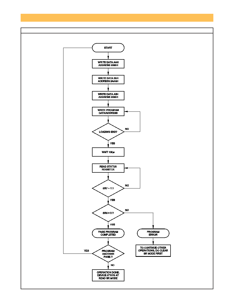
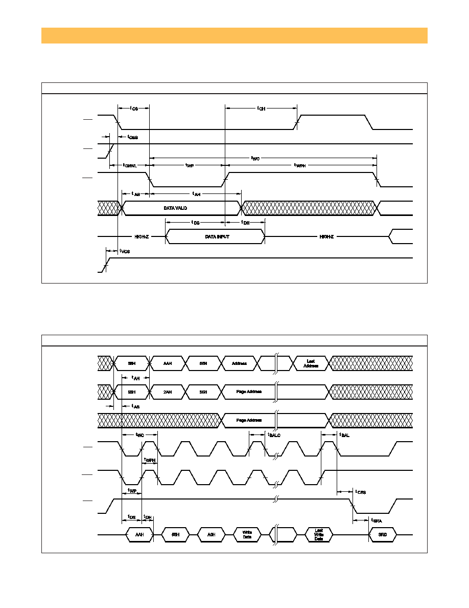
PAGE PROGRAM
To initiate Page Program mode, a three-cycle command sequence
is required. There are two "unlock" write cycles. These are
followed by writing the page program command - A0H.
After three-cycle command sequence is given, a word load is
performed by applying a low pulse on the WE or CE input with CE
or WE low (respectively) and OE high. The address is latched on
the falling edge of CE or WE, whichever occurs last. The data is
latched by the first rising edge of CE or WE. Maximum of 64 words
of data may be loaded into each page by the same procedures as
outlined in the page program section below.
WORD LOAD
Word loads are used to enter the 64 words of a page to be
programmed. A word load is performed by applying a low pulse on
the WE or CE input CE or WE low respectively) and OE high. The
address is latched on the falling edge of CE or WE, whichever
occurs last. The data is latched by the first rising edge of CE or
WE.
PROGRAM
Any page to be programmed should have the page in the erase
state first, i.e. performing sector erase is suggested before page
programming can be performed.
The device is programmed on a page basis. If a word of data within
a page is to be changed, data for the entire page can be loaded into
the device. Any word that is not loaded during the programming of
its page will be still in the erase state (i.e. FFFFH). Once the words
of a page are loaded into the device, they are simultaneously
programmed during the internal programming period. After the first
data word has been loaded into the device, successive words are
entered in the same manner. Each new word to be programmed
must have its high to low transition on WE (or CE) within 30
µ
s of
the low to high transition of WE (or CE) of the preceding word. A6
to A19 specify the page address, i.e. the device is page-aligned on
64 word boundary The page address must be valid during each
high to low transition of WE or CE. A0 to A5 specify the word
address within the page. The word may be loaded in any order;
sequential loading is not required. If a high to low transition of CE
or WE is not detected within 100
µ
s of the last low to high transition,
the load period will end and the internal programming period will
start. The auto page program terminates when status on I/O7 is "1"
at which time the device stays at read status register mode until the
CIR contents are altered by a valid command sequence. (Refer to
Table 2 & 5 and Figure 1, 6 & 7)
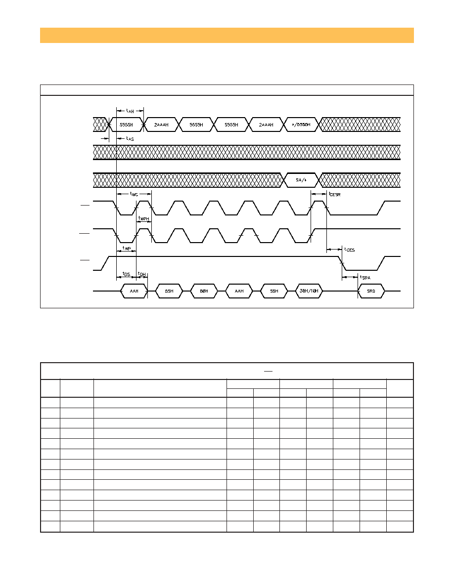
CHIP ERASE
Chip erase is a six-bus cycle operation. There are two "unlock"
write cycles. These are followed by writing the "set-up" command -
80H. Two more "unlock" write cycles are then followed by the chip
erase command - 10H.
Chip erase does not require the user to program the device prior to
erase.
The automatic erase begins on the rising edge of the last WE pulse
in the command sequence and terminates when the status on I/O7
(I/O23) is "1" at which time the device stays at read status register
mode until the CIR contents are altered by a valid command
sequence. (Refer to Tables 2 & 5 and Figures 2, 6 & 8).
SECTOR ERASE
Sector erase is a six-bus cycle operation. There are two "unlock"
write cycles. These are followed by writing the set-up command -
80H. Two more "unlock" write cycles are then followed by the
sector erase command - 30H. The sector address is latched on the
falling edge of WE, while the command (data) is latched on the
rising edge of WE.
Sector erase does not require the user to program the device prior
to erase. The system is not required to provide any controls or
timings during these operations.
The automatic sector erase begins on the rising edge of the last WE
pulse in the command sequence and terminates when the status on
I/O7 (I/O23) is "1" at which time the device stays at read status
register mode. The device remains enabled for read status register
mode until the CIR contents are altered by a valid command
sequence. (Refer to Tables 2, & 5 and Figures 3, 4, 6 & 8).
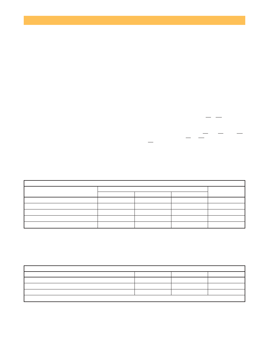
Table 4: Sector Address*
A19
A18
A17
A16
Address Range
[A0 - A15]
SA0
0
0
0
0
00000H--0FFFFH
SA1
0
0
0
1
10000H--1FFFFH
SA2
0
0
1
0
20000H--2FFFFH
SA3
0
0
1
1
30000H--3FFFFH
SA4
0
1
0
0
40000H--4FFFFH
...
....
...
...
................
SA15
1
1
1
1
F0000H--FFFFFH
* Per 1 Meg x 16 device.
ERASE SUSPEND
This command only has meaning while the WSM is executing
SECTOR or CHIP erase operations, and therefore will only be
responded to during SECTOR or CHIP erase operation. After this
command has been executed, the CIR will initiate the WSM to
suspend erase operations, and then return to Read Status Register
mode. The WSM will set the I/O6 bit to a "1". Once the WSM has
reached the Suspend state, the WSM will set I/O7 (I/O23) bit to a
"1". At this time, WSM allows CIR to respond to the Read Array,
Read Status Register, Abort and Erase Resume commands only. In
this mode, the CIR will not respond to any other commands. the
WSM will continue to run, idling in the SUSPEND state, regardless
of the state of all input control pins.
ERASE RESUME
This command will cause the CIR to clear the suspend state and set
the I/O6 (I/O22) to a "0", but only in an Erase Suspend command
was previously used. Erase Resume will not have any effect in all
other conditions.
READ STATUS REGISTER COMMAND
The module contains a Status Register which may be read to
determine when a program or erase operation is complete, and
whether that operation completed successfully. The status register
may be read at any time by writing the Read Status command to the
CIR. After writing this command, all subsequent read operations
output data from the status register, until another valid command is
written to the CIR. A Read Array command must be written to the
CIR to return to the Read Array mode.
The status register bits are output on I/O2 - I/O7 (I/O18 - I/O23)
(Table 5), I/O0 - I/O1 (I/O16 - I/O17) is set to 0H.
It should be noted that the status register are latched on the falling
edge of OE or CE whichever occurs last in the read cycle. This
prevents possible bus errors which might occur if the contents of the
status register change while reading the status register. CE or WE
must be toggled with each subsequent status read, or the
completion of a program or erase operation will not be evident.
30A180-11
www.dpactech.com
5
Rev. D 5/02
32 Megabit FLASH EEPROM
DP5Z1MW32PV3
The Status Register is the interface between the microprocessor
and the Write State Machine (WSM). When the WSM is active, this
register will indicate the status of the WSM, and will also hold the
bits indicating whether or not the WSM was successful in
performing the desired operation. The WSM sets status bits four
through seven and clears bits six and seven, but cannot clear status
bits four and five. If Erase fail or Program fail status bit is detected,
the Status Register is not cleared until the Clear Status Register
command is written. The device automatically outputs Status
Register data when read after Chip Erase, Sector Erase, Page
Program or Read Status Command write cycle. the default state of
the Status Register after power-up is (I/O7 - I/O4 and I/O23 - I/O20)
= 1000B. I/O3 and I/O19 = 0 or 1 depends on sector-protect status,
can not be changed by Clear Status Register Command or Write
State Machine. I/O2 and I/O16 = 0 or 1 depends on Sleep status,
During Sleep mode or Abort mode I/O2 (I/O18) is set to "1"; I/O2
(I/O18) is reset to "0" by Read Array command.
CLEAR STATUS REGISTER
The Erase fail status bit (I/O5 and I/O21) and Program fail status bit
(I/O4 and I/O20) are set by the write state machine, and can only
be reset by the system software. These bits can indicate various
failure conditions (see Table 5). By allowing the system software to
control the resetting of these bits, several operations may be
performed (such as cumulatively programming several pages or
erasing multiple blocks in sequence). The Status register may then
be read to determine if an error occurred during that programming
or erasing series. This adds flexibility to the way the device may be
programmed or erased. Additionally, once the program (erase) fail
bit happens, the program (erase) operation can not be performed
further. The program (erase) fail bit must be reset by system
software before further page program or sector (chip) erase are
attempted. To clear the status register, the Clear Status Register
command is written to the CIR. Then, any other command may be
issued to the CIR. Note again that before a read cycle can be
initiated, a Read command must be written to the CIR to specify
whether the read data is to come from the Array, Status Register or
Silicon ID.
SLEEP MODE
The device features two software controlled low-power modes:
Sleep and Abort modes. Sleep mode is allowable during any
current operations except that once Suspend command is issued,
Sleep command is ignored. Abort mode is executed only during
page Programming and Chip/Sector Erase mode.
To activate Sleep mode, a three-bus cycle operation is required.
C0H command (refer to Table 2) puts the device in the Sleep mode.
Once in the Sleep mode and CMOS input level applied, the power
of the device is reduced to deep power-down current levels. The
only threshold condition, input leakage, and output leakage.
The Sleep command allows the device to COMPLETE current
operations before going into Sleep mode. Once current operation is
done, device stays at read status register mode. The status
registers are not reset during sleep command. Program or Erase
fail bit may have been set if during program/erase mode the device
retry exceeds maximum count.
During Sleep mode, the status registers, Silicon ID codes remain
valid and can still be read. The device Sleep Status bit - I/O2
(I/O18) will indicate that the device in the sleep mode.
Write and Read Array command wakes up the device out of Sleep
mode, I/O2 (I/O18) is reset to "0" and device returns to standby
current level.
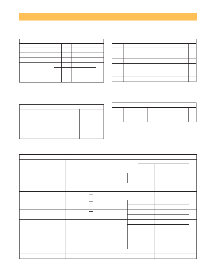
Table 5: Status Register
11
STATUS
I/O7
(I/O23)
I/O6
(I/O22)
I/O5
(I/O21)
I/O4
(I/O20)
I/O3
(I/O19)
I/O2
(I/O18)
IN PROGRESS
PROGRAM
a, b, f
0
0
0
0
1/01/0
1/0
ERASE
a, c, f
0
0
0
0
1/0
1/0
SUSPEND (NOT COMPLETE)
a, d, f
0
1
0
0
1/0
1/0
SUSPEND (COMPLETE)
a, d, f
1
1
0
0
1/0
1/0
COMPLETE
PROGRAM
a, b, f
1
0
0
0
1/0
1/0
ERASE
a, c, f
1
0
0
0
1/0
1/0
FAIL
PROGRAM
a, e, f
1
0
0
1
1/0
1/0
ERASE
a, e, f
1
0
1
0
1/0
1/0
AFTER CLEARING STATUS REGISTER
f
1
0
0
0
1/0
Note `g'
NOTES:
a. I/O7, I/O23: Write State Machine Status
1 = Ready, 0 = Busy
I/O6, I/O22: Erase Suspend Status
1 = Suspend, 0 = No Suspend
I/O5, I/O21: Erase Fail Status
1 = Fail in Erase, 0 = Successful Erase
I/O4, I/O20: Program Fail Status
1 = Fail in Program, 0 = Successful Program
I/O3, I/O19: Sector-Protect Status (Not Used)
I/O2, I/O18: Sleep Status
1 = Device in Sleep Status, 0 = Device Not in Sleep Status
I/O1-I/O0, I/O17-I/O16 = Reserved for further enhancements.
These bits are reserved for future use; mask them out when polling
the Status Register.
b. Program Status is for the status during Page Programming mode.
c. Erase Status is for the status during Sector/Chip Erase mode.
d. Suspend Status is for both Sector and Chip Erase mode.
e. Fail Status bit (I/O4, I/O20 or I/O5,I/O21) is provided during Page
Program or Sector/Chip Erase modes respectively.
f.
I/O2, I/O18 = 0 or 1 depends on whether device is in the Sleep
mode or not.
g. Once in the Sleep mode, I/O2, I/O18 is set to "1", and is reset by
read array command only.
30A180-11
www.dpactech.com
6
Rev. D 5/02
32 Megabit FLASH EEPROM
DP5Z1MW32PV3
ABORT MODE
To activate Abort mode, a three-bus cycle operation is required.
The E0H command (refer to Table 3) only stops page program or
Sector/Chip erase operations currently in progress and puts the
device in Sleep mode. But unlike the Sleep command, the program
or erase operation will not be completed. Since the data in some
page/sectors is no longer valid due to an incomplete program or
erase operation, the program fail bit I/O4 (I/O20) or erase fail bit
I/O5 (I/O21) will be set.
After the abort command is executed and with CMOS input levels
applied, the device current is reduced to the same level as in deep
power-down or sleep modes. Device stays at read register mode.
During Abort mode, the status register, Silicon ID codes remain
valid and can still be read. The device Sleep Status bit - I/O2
(I/O18) will indicate that the device in the sleep mode.
DATA PROTECTION
The device is designed to offer protection against accidental
erasure or programming caused by spurious system level signals
that may exit during power transitions. During power-up the device
automatically resets the internal state machine in the read array
mode. Also, with its control register architecture, alterations of the
memory contents only occurs after successful completion of
specific multi-bus cycles command sequences.
the device also incorporates several features to prevent inadvertent
write cycles resulting from V
DD
power-up and power-down
transitions or system noise.
LOW V
DD
WRITE INHIBIT
To avoid initiation of a write cycle during V
DD
power-up and
power-down, a write cycle is locked out for V
DD
less than V
OKL
(=3.2V, typically 3.5V). If V
DD
< V
LKO
, the command register is
disabled and all internal program/erase circuits are disabled. Under
this condition the device will reset to the read mode. Subsequent
writes will be ignored until the V
DD
level is greater than VLKO. It is
logically correct to prevent unintentional write when V
DD
is above
V
LKO
.
WRITE PULSE "GLITCH" PROTECTION
Noise pulses of less than 10ns (typical) on CE or WE will not initiate
a write cycle.
LOGICAL INHIBIT
Writing is inhibited by holding any one of OE = V
IL
, CE = V
IH
or WE
= V
IH
. To initiate a write cycle CE and WE must be a logical zero
while OE is a logical one.
ERASE PROGRAMMING PERFORMANCE*
PERAMETER
LIMITS
UNITS
MIN.
TYP.
MAX.
Chip/Sector Erase Time
150
2000
ms
Page Programming Time
3
60
ms
Chip Program Time *
48
150
sec
Erase/Program Cycles
10,000
Cycles
Byte Program Time
24
µ
s
* Per 1 Meg x 16 device.
LATCH UP CHARACTERISTICS
PARAMETER
MIN.
MAX.
UNITS
Input Voltage with Respect to V
SS
on all pins except I/O pins
-1.0
13.5
V
Input Voltage with Respect tn V
SS
on all I/O pins
-1.0
V
DD
+1.0
V
Current
-100
+100
mA
Includes all pins except V
DD
. Test Conditions:
V
DD
5.0V, one pin at a time
30A180-11
www.dpactech.com
7
Rev. D 5/02
32 Megabit FLASH EEPROM
DP5Z1MW32PV3
RECOMMENDED OPERATING RANGE
1
Symbol
Characteristic
Min.
Typ.
Max.
Unit
V
DD
Supply Voltage
4.5
5.0
5.5
V
V
IL
Input Low Voltage
-0.5
2
0.8
V
V
IH
Input HIGH Voltage
2.0
V
DD
+0.5
V
T
A
Operating
Temperature
C
0
+25
+70
∞
C
I
-40
+25
+85
M/B
-55
+25
+125
V
ID
A9 I.D. Input/Output
11.5
12.5
V
CAPACITANCE
5
: T
A
= +25 C, F = 1.0MHz
Symbol
Parameter
Max.
Condition
Unit
C
ADR
Address Input
35
V
IN
2
= 0V
pF
C
CE
Chip Enable
25
C
WE
Write Enable
35
C
OE
Output Enable
35
C
I/O
Data Input/Output
30
ABSOLUTE MAXIMUM RATINGS
5
Symbol
Parameter
Calue
Unit
T
STG
Storage Temperature
-65 to +125
∞
C
T
BIAS
Temperature Under Bias
-55 to +125
∞
C
T
OP
Operating Temperature
-55 to 125
∞
C
I
OUT
Output Short
Circuit Current
100
4
mA
V
I/O
Input/Output Voltage
1
-0.5 to 7.0
2
V
V
DD
Supply Voltage
1
-0.5 to 7.0
3
V
DC OUTPUT CHARACTERISTICS
Symbol
Parameter
Condition
Min.
Max.
Unit
V
OH
HIGH Voltage
I
OH
= -400
µ
A
2.4
V
V
OL
LOW Voltage
9
I
OL
= 2.1 mA
0.45
V
DC CHARACTERISTICS:
Over Operating Ranges
Symbol
Characteristics
Test Conditions
Limits
Unit
Min.
Typ.
Max.
I
IL
Input Load Current
6
V
DD
= V
DD
max., V
IN
= V
DD
or V
SS
-20
+20
µ
A
I
OL
Output
Leakage Current
6
V
DD
= V
DD
max., V
IN
= V
DD
or V
SS
x16
-20
+20
µ
A
x32
-10
+10
I
SB1
V
DD
Standby
Current (CMOS)
V
DD
= V
DD
max., CE = V
DD
±
0.2V
100
400
µ
A
I
SB2
V
DD
Standby
Current (TTL)
6
V
DD
= V
DD
max., CE = V
IH
4
42
µ
A
I
CC1
V
DD
Read current
V
DD
= V
DD
max., CE = V
IL
,
Inputs - V
IL
or V
IH
, f = 10MHz, I
OUT
= 0mA
x16
55
85
mA
x32
100
160
I
CC2
V
DD
Read Current
6
V
DD
= V
DD
max., CE = V
IL
,
Inputs - V
IL
or V
IH
, f = 5MHz, I
OUT
= 0mA
x16
35
50
mA
x32
60
90
I
CC3
V
DD
Erase
Suspend Current
6, 8
Block Erase in Suspend, CE = V
IH
x16
10
25
mA
x32
10
40
I
CC4
V
DD
Program Current
6
Program in Progress
x16
35
65
mA
x32
60
120
I
CC5
V
DD
Erase Current
Erase in Progress
x16
35
6
mA
x32
60
120
V
IL
Input Low Voltage
9
-3.0
0.8
V
V
IH
Input High Voltage
2.4
V
DD
+3.0
V
30A180-11
www.dpactech.com
8
Rev. D 5/02
32 Megabit FLASH EEPROM
DP5Z1MW32PV3
FIGURE 1: AUTOMATIC PAGE PROGRAM FLOW CHART
11
NOTE: SR = Status Register

30A180-11
www.dpactech.com
9
Rev. D 5/02
32 Megabit FLASH EEPROM
DP5Z1MW32PV3
FIGURE 2: AUTOMATIC CHIP ERASE FLOW CHART
11

30A180-11
www.dpactech.com
10
Rev. D 5/02
32 Megabit FLASH EEPROM
DP5Z1MW32PV3
FIGURE 3: AUTOMATIC SECTOR ERASE FLOW CHART
11

30A180-11
www.dpactech.com
11
Rev. D 5/02
32 Megabit FLASH EEPROM
DP5Z1MW32PV3
FIGURE 4: ERASE SUSPEND/ERASE RESUME FLOW CHART
11

30A180-11
www.dpactech.com
12
Rev. D 5/02
32 Megabit FLASH EEPROM
DP5Z1MW32PV3
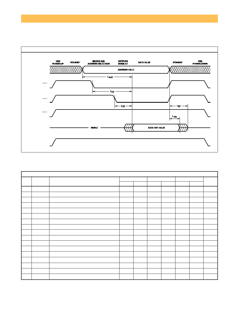
AC TEST CONDITIONS
Input Pulse Levels
0.45V to 2.4V
Input Pulse Rise and Fall Times
10ns
Input and Output Timing
Reference Levels
0.8V, 2.0V
OUTPUT LOAD
Load
C
L
Parameters Measured
1
100pF
except t
DF
, t
LZ
and t
OLZ
2
30pF
t
DF
, t
LZ
and t
OLZ
AC INPUT/OUTPUT REFERENCE WAVEFORM
OUTPUT LOAD
DEVICE
UNDER
TEST
1.8K
+5V
C
L
*
6.2K
DIODES = IN3064 or Equivalent
* Including Probe and Jig Capacitance.
AC Operating Conditions and Characteristics - READ CYCLE: Over operating ranges
No.
Symbol
Parameter
120ns
150ns
200ns
Unit
Min.
Max.
Min.
Max.
Min.
Max.
1
t
ACC
Address to Output Delay
120
120
150
ns
2
t
CE
Chip Enable Output Delay
120
120
150
ns
3
t
OE
Output Enable Output Delay
60
70
70
ns
4
t
DF
Output Enable to Output Delay
0
55
0
55
0
ns
5
t
OH
Address to Output Hold
0
0
0
ns
30A180-11
www.dpactech.com
13
Rev. D 5/02
32 Megabit FLASH EEPROM
DP5Z1MW32PV3
Figure 5: READ CYCLE
ADDRESS
CE
OE
WE
DATA I/O
V
DD
AC Operating Conditions and Characteristics - WRITE/ERASE/PROGRAM CYCLE: Over operating ranges
No.
Symbol
Parameter
120ns
150ns
200ns
Unit
Min.
Max.
Min.
Max.
Min.
Max.
6
t
WC
Write Cycle Time
120
150
200
ns
7
t
AS
Address Setup Time
0
0
0
ns
8
t
AH
Address Hold Time
50
60
70
ns
9
t
DS
Data Setup Time
50
60
70
ns
10
t
DH
Data Hold Time
10
10
10
ns
11
t
OES
Output Enable Setup Time
0
0
0
ns
12
t
CES
Chip Enable Setup Time
0
0
0
ns
13
t
GHWL
Read Recovery Time before Write
0
0
0
ns
14
t
CS
Chip Enable Setup Time
0
0
0
ns
15
t
CH
Chip Enable Hold Time
0
0
0
ns
16
t
WP
Write Pulse Width
50
60
70
ns
17
t
WPH
Write Pulse Width HIGH
50
50
50
ns
18
t
BALC
Byte Address Load Cycle
0.3
30
0.3
30
0.3
30
µ
s
19
t
BAL
Byte Address Load Time
100
100
100
µ
s
20
t
SRA
Status Register Access Time
120
150
200
ns
21
t
CESR
Chip Enable Setup before SR Read
100
100
100
ns
22
t
VCS
V
DD
Setup Time
2
2
2
µ
s
30A180-11
www.dpactech.com
14
Rev. D 5/02
32 Megabit FLASH EEPROM
DP5Z1MW32PV3
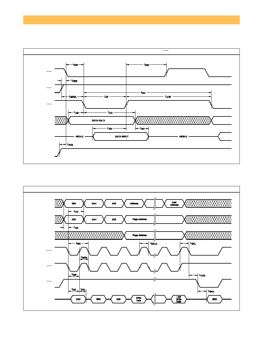
Figure 7: AUTOMATIC PAGE PROGRAM CYCLE
10
Figure 6: WRITE CYCLE
A0 - A5
A6 - A14
A15 - A19
CE
WE
OE
DATA I/O
CE
OE
WE
ADDRESS
DATA I/O
V
DD
30A180-11
www.dpactech.com
15
Rev. D 5/02
32 Megabit FLASH EEPROM
DP5Z1MW32PV3
AC Operating Conditions and Characteristics:
Over operating ranges
WRITE/ERASE/PROGRAM OPERATION ALTERNATE CE CONTROLLED WRITES
No.
Symbol
Parameter
120ns
150ns
200ns
Unit
Min.
Max.
Min.
Max.
Min.
Max.
23
t
WC
Write Cycle Time
120
150
200
ns
24
t
AS
Address Setup Time
0
0
0
ns
25
t
AH
Address Hold Time
50
60
70
ns
26
t
DS
Data Setup Time
50
60
70
ns
27
t
DH
Data Hold Time
10
10
10
ns
28
t
OES
Output Enable Setup Time
0
0
0
ns
29
t
CES
Chip Enable Setup Time
0
0
0
ns
30
t
GHWL
Read Recovery Time before Write
0
0
0
ns
31
t
WS
Write Enable Setup Time
0
0
0
ns
32
t
WH
Write Enable Hold Time
0
0
0
ns
33
t
CP
Chip Enable Pulse Width
50
60
70
ns
34
t
CPH
Chip Enable Pulse Width HIGH
50
50
50
ns
35
t
VCS
V
DD
Setup Time
2
2
2
µ
s
Figure 8: AUTOMATIC SECTOR/CHIP ERASE CYCLE
A0 - A14
A15
A16 - A19
CE
WE
OE
DATA I/O
30A180-11
www.dpactech.com
16
Rev. D 5/02
32 Megabit FLASH EEPROM
DP5Z1MW32PV3
Figure 10: AUTOMATIC PAGE PROGRAM TIMING CYCLE
10
A0 - A5
A6 - A14
A15 - A19
WE
CE
OE
DATA I/O
Figure 9: COMMAND WRITE CYCLE
(Alternate CE Controlled)
WE
OE
CE
ADDRESS
DATA I/O
V
DD

30A180-11
www.dpactech.com
17
Rev. D 5/02
32 Megabit FLASH EEPROM
DP5Z1MW32PV3
NOTES:
1. All voltages are with respect to V
SS
.
2. -2.0V min. for pulse width less than 20ns (V
IL
min. = -0.5V at DC level).
3. Maximum DC voltage on V
PP
or A9 may over shoot to +14.0V for periods less than 20ns.
4. Stresses greater than those under ABSOLUTE MAXIMUM RATINGS may cause permanent damage to the device. This is a stress rating only
and functional operation of the device at these or any other conditions above those indicated in the operational sections of this specification is
not implied. Exposure to absolute maximum rating conditions for extended periods may affect reliability.
5. This parameter is guaranteed and not 100% tested.
6. All currents are in RMS unless otherwise noted. Typical values at V
DD
= 5.0V, t = 25
∞
C. These currents are valid for all product versions
(package and speeds.).
7. I
CC3
is specified with the device de-selected. If the device is read while in erase suspend mode,
current draw is the sum of I
CC3
and I
CC1
/I
CC2
.
8. V
IL
min. = -1.0V for pulse width
50ns.
9. V
IL
min. = -2.0V for pulse width
20ns.
10. Refer to page 5 for detail Page Program Operation.
11. Each SLCC contains one 1 Meg x 16 FLASH memory device enabled by separate chip enables. Typically the module is used as a x32 device.
When writing commands to the command register (CIR) under these conditions, the command sequence shown in the command definition
table should be duplicated to each word (I/O0 - I/O15 and I/O16 - I/O31) of the module. The command sequence for a Read/Reset cycle would
be as follows: On the first bus cycle XXAAXXAAH would be written to Address 5555H, on the second bus cycle XX55XX55H would be written to
address 2AAAH followed on the third bus cycle by XXF0XXF0H being written to address 5555H (in this example X = Don't Care). A single
device can be programmed by writing the appropriate command sequence to that device while writing the Read/Rest command sequence to
the other enabled device.
12. FAH is the device identification for Macronix Revision A die (MX29F1610AHC). F1H is the device identification for Macronix non-revision die
(MX29F1610HC).
WAVEFORM KEY
Data Valid
Transition from
Transition From
Data Undefined
HIGH to LOW
LOW to HIGH
or Don't Care
30A180-11
www.dpactech.com
18
Rev. D 5/02
32 Mega bit FLASH EEPROM
DP5Z1MW32PV3
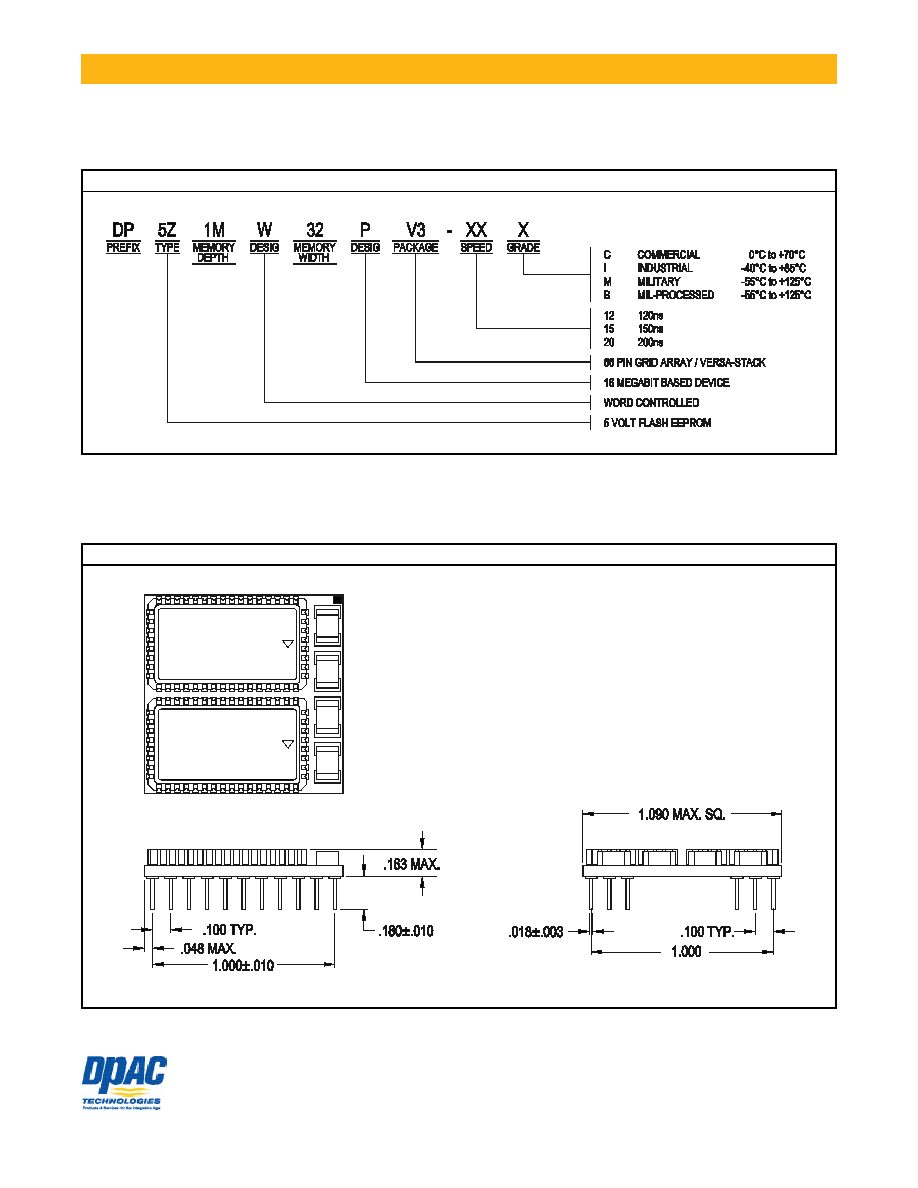
ME CHAN I CAL DRAWING
OR DERING INFORMATION
DPAC Technologies Products & Services for the Integration Age
7321 Lincoln Way, Garden Grove, CA 92841 Tel 714 898 0007 Fax 714 897 1772
www.dpactech.com Nasdaq: DPAC
©2002 DPAC Technologies, all rights reserved. DPAC TechnologiesTM, Versa-StackTM, LP-StackTM, CS StackTM are trademarks of DPAC Technologies Corp.