PRELIMINARY
DESCRIPTION:
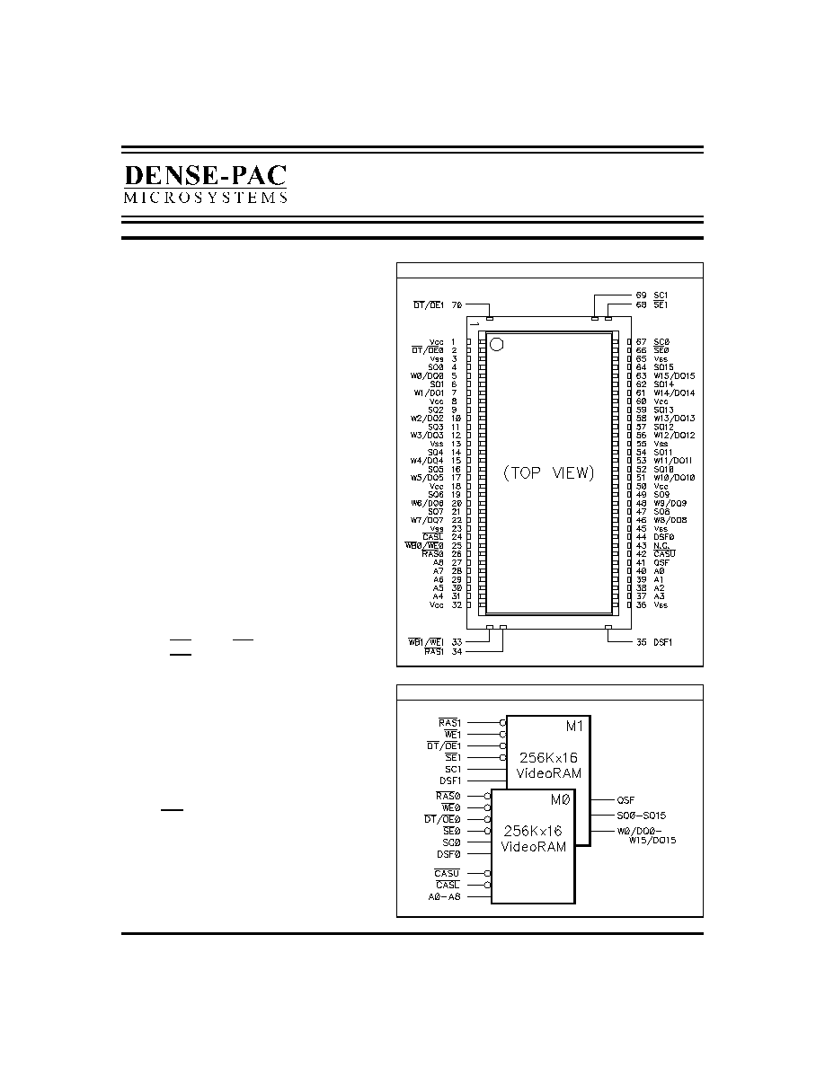
The DPO512X16MGY5-CM is a 512Kx16 bit Dual
Port Dynamic RAM module that utilize the new and
innovative space saving SOP stacking technology.
The module is constructed of two Samsung©
256Kx16 CMOS Video RAMs each consists of
256Kx16 Dynamic Random Access Memory (RAM)
port and 512Kx16 Static Serial Access Memory
(SAM) port. The RAM and SAM port operate
asynchronously except during data transfer between
the ports.
The DPO512X16MGY5-CM provides for a
compatible upgrade path to higher density
compatible modules.
FEATURES:
∑
Access Times (DRAM/SAM):
50/15, 60/15, 70/17ns (max.)
∑
Dual Port Video RAM
∑
Two 256Kx16 DRAM, 512Kx16 SAM
with Individual Control
∑
Screened to -55
∞
C to +125
∞
C
∑
Single 5.0
±
10% Supply Voltage, TTL Interface
∑
512 Cycle/8ms Refresh
∑
Three Variations of Refresh:
CAS-Before-RAS
RAS-Only
Hidden Refresh
∑
Fast Page Mode with Extended Data Out
∑
RAM Read, Write, Read-Modify-Write
∑
Serial Read (SR)
∑
Split Read Transfer with Stop Operation (SRT)
∑
Read/Real Time Read Transfer (RT,RRT)
∑
Eight Column Block Write (BW) and Write per
Bit with Masking Operation (New & Old Mask)
∑
Dual CAS Byte/Word Read/Write Operation
∑
Common Data Inputs and Outputs Using three
state RAM Output Control
∑
All Inputs and Outputs TTL Compatible
∑
M-Densus
Package:
70-Pin Leadless Stack
PIN-OUT DIAGRAM
FUNCTIONAL BLOCK DIAGRAM
16Mx36, 50 - 70ns, TSTACK
30A165-33
B
This document contains information on a product presently under
development at Dense-Pac Microsystems, Inc. Dense-Pac reserves the
right to change products or specifications herein without prior notice.
8 Megabit
CMOS VIDEO RAM
DPO512X16MGY5-CM
M-Densus
High Density Memory Device
30A209-00
REV. A
1

DPO512X16MGY5-CM
Dense-Pac Microsystems, Inc.
PRELIMINARY
PIN NAMES
A0 - A8
Address inputs for the DRAM operation, these inputs are multiplexed and clocked by RAS and
CAS to select one 16 bit word out of the 262,144 available per device. Nine row address bits are
latched on the falling edge of the row address strobe (RAS) and the following nine column
address bits are latched on the falling edge of the column address strobe.
W0/DQ0 - W15/DQ15
Data In / Data Out for DRAM access. These pins act as inputs for Mask and register load cycles,
DQ Mask and Column Mask for BW.
SQ0 - SQ15
Serial output pin for serial read. (Serial write is not supported)
CASL, CASU
Column Address Strobes. CASL, CASU are used to clock in the nine column address bits as a
strobe forth DSF inputs and used to Byte/Word Read, Write Operations.
RAS0, RAS1
Row Address Strobe. RAS is used to clock the nine row bits for another input signal. The RAM
port is placed in standby mode when the RAS control is held "High".
WB0/WE0, WB1/WE1
Data Write Enable. WB/WE input is a multi-function pin. When WB/WE is "High" at the falling
edge of RAS, during RAM port operation, it is used to write data into the memory array in the
same as a standard DRAM. When WB/WE is "Low" at the falling edge of RAS, during RAM port
operation, the W-P-B function is enabled.
DT0/OE0, DT1/OE1
The DT/OE input is also a multi function pin. Enables and internal Transfer Operation at the
falling edge of RAS when Transfer is enabled.
SE0, SE1
In serial read cycles , SE is used as an output control. When SE is "High", serial access is
disabled, however, the serial address pointer is still incremented while SC is clocked.
SC0, SC1
Clock input to the serial address counter and data latch for the SAM register.
DSF0, DSF1
DSF is used to indicate which special functions (VW, FW, Split Transfer, etc.) are used for a
particular access cycle.
QSF
QSF indicated which half of the SAM is being accessed. Low if address is 0 - 255, High if address
is 256 - 511.
V
CC
Power Supply (+5.0V)
V
SS
Ground
N.C.
No Connect
RECOMMENDED OPERATING CONDITIONS
Symbol
Parameter
Min.
Typ.
Max.
Units
V
CC
Supply Voltage
4.5
5.0
5.5
V
V
SS
Ground
0
0
0
V
V
IL
Input Low Voltage
-2.4
-
V
CC
+1.0V
V
V
IH
Input High Voltage
-1.0
-
0.8
V
CAPACITANCE:
V
CC
= 5.0V, T
A
= 25
o
C, f = 1MHz *
Symbol
Parameter
Min.
Max.
Unit
C
IN1
Input Capacitance: A0 - A8
4
12
pF
C
IN2
Input Capacitance: CASU, CASL, DSF
4
14
pF
C
IN3
Input Capacitance: SC, SE, DT/OE, RAS, WB/WE
2
7
pF
C
DQ
Input/Output Capacitance: W0/DQ0 - W15/DQ15
4
14
pF
C
SQ
Output Capacitance: SQ0 - SQ15, QSF
4
14
pf
* Values calculated not measured.
30A209-00
REV. A
2
Dense-Pac Microsystems, Inc.
DPO512X16MGY5-CM
PRELIMINARY
ABSOLUTE MAXIMUM RATINGS
Symbol
Parameter
Value
Units
T
STC
Storage Temperature
-55 to +150
o
C
V
IN
Input Voltage on Any Pin Relative to V
SS
-1.0 to +7.0
V
V
OUT
Output Voltage on Any Pin Relative to V
SS
-1.0 to +7.0
V
V
CC
V
CC
Supply Voltage
-1.0 to +7.0
V
P
D
Power Dissipation
1
W
I
OS
Short Circuit Output Current
50
mA
NOTE: Permanent device damage may occur of "ABSOLUTE MAXIMUM RATINGS" are exceeded. Functional operation should be restricted to the
conditions as detailed in the operational sections of the component data sheet (Samsung KM4216C528). Exposure to absolute maximum rating
conditions for extended periods may affect device reliability.
DC OPERATING CHARACTERISTICS
Symbol
Characteristic
1
RAM Port
SAM Port
50ns
60ns
70ns
Units
I
CC1
Operating Current
RAS and CAS cycling
@ t
RC
= min.
Standby
2
140
130
120
mA
I
CC1
A
Active
180
170
155
I
CC2
Standby Current
RAS, CAS, DT/OE, WB/WE = V
IH
,
DSF = V
IL
Standby
2
20
20
20
mA
I
CC2
A
Active
65
60
55
I
CC3
RAS - Only Refresh
Current
CAS = V
IH
,
RAS Cycling @ t
RC
= min.
Standby
2
140
130
120
mA
I
CC3
A
Active
180
170
155
I
CC4
Extended Fast Page
Mode Current
RAS = V
IL
,
CAS Cycling @ t
RC
= min.
Standby
2
140
130
120
mA
I
CC4
A
Active
180
170
155
I
CC5
CAS - Before - RAS
Refresh Current
RAS and CAS Cycling
@ t
RC
= min.
Standby
2
140
130
120
mA
I
CC5
A
Active
180
170
155
I
CC6
Data Transfer
Current
RAS and CAS Cycling
@ t
RC
= min.
Standby
2
170
150
140
mA
I
CC6
A
Active
200
190
175
I
CC7
Block Write Cycle
Current
RAS and CAS Cycling
@ t
RC
= min.
Standby
2
140
130
120
mA
I
CC7
A
Active
180
170
155
I
CC8
Color Register
Load Current
RAS and CAS Cycling
@ t
RC
= min.
Standby
2
130
120
100
mA
I
CC8
A
Active
180
150
135
1.
Real values depend on output loading and cycle rates. Specified values are obtained with the output open. I
CC
is specified as
average current. In I
CC1
, I
CC3
, I
CC6
, I
CC7
, I
CC8
, address transition should be changed only once while RAS = V
IL
. In I
CC4
, address transition
should be changed only once while CAS = V
IH
.
2. SAM standby condition: SE
V
IH
, SC
V
IL
or
V
IH
.
INPUT/OUTPUT CURRENT:
Recommended Operating Conditions unless otherwise specified
Symbol
Parameter
Conditions
Min.
Max.
Unit
I
IL
Input
Leakage Current
Any Input 0
V
IN
V
CC
+0.5V, All other
pins not under test = 0 Volts
-20
+20
µ
A
I
OL
Output Leakage Current
Data out is disabled, 0
V
OUT
V
CC
-20
+20
µ
A
V
OH
Output High Voltage Level
RAM I
OL
= -2mA, SAM I
OL
= -2mA
2.4
-
V
V
OL
Output Low Voltage Level
RAM I
OL
= 2mA, SAM I
OL
= 2mA
-
0.4
V
30A209-00
REV. A
3

DPO512X16MGY5-CM
Dense-Pac Microsystems, Inc.
PRELIMINARY
For additional operating, electrical and timing information see device manufacturers data sheet for Samsung part number
KM4216C258 located at: http://www.usa.samsungsemi.com/products/prodspec/videoram/4216c258.pdf
Dense-Pac Microsystems, Inc.
7321 Lincoln Way Garden Grove , California 92841-1431
(714) 898-0007 (800) 642-4477
(Outside CA)
FAX: (714) 897-1772 http://www.dense-pac.com
MECHANICAL DRAWING
ORDERING INFORMATION
30A209-00
REV. A
4