VENTURA
32 Megabit High Speed CMOS SRAM
DPS2MX16MKn3
DESCRIPTION:
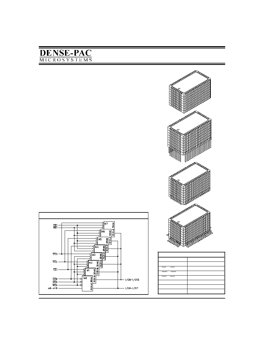
The DPS2MX16MKn3 High Speed SRAM `'STACK'' modules are
a revolutionary new memory subsystem using Dense-Pac
Microsystems' ceramic Stackable Leadless Chip Carriers (SLCC).
Available in straight leaded, `'J'' leaded or gullwing leaded
packages. The module packs 32-Megabits of low-power CMOS
static RAM in an area as small as 0.549 in
2
, while maintaining a
total height as low as 0.545 inches.
The DPS2MX16MKn3 STACK modules contain eight individual
512K x 8 SRAMs, each packaged in a hermetically sealed SLCC,
making the modules suitable for commercial, industrial and
military applications.
By using SLCCs, the `'Stack'' family of modules offer a higher
board density of memory than available with conventional
through-hole, surface mount or hybrid techniques.
FEATURES:
·
Organizations Available: 2 Meg x 16
·
Access Times: 20*, 25, 30, 35, 45ns
·
Fully Static Operation - No clock or refresh required
·
Single +5V Power Supply,
±
10% Tolerance
·
TTL Compatible
·
Common Data Inputs and Outputs
·
Low Data Retention Voltage: 2.0V min.
·
Packages Available:
SLCC Stack
Straight Leaded Stack
`'J'' Leaded Stack
Gullwing Leaded Stack
*
Commercial and Industrial Grade only.
FUNCTIONAL BLOCK DIAGRAM
PIN NAMES
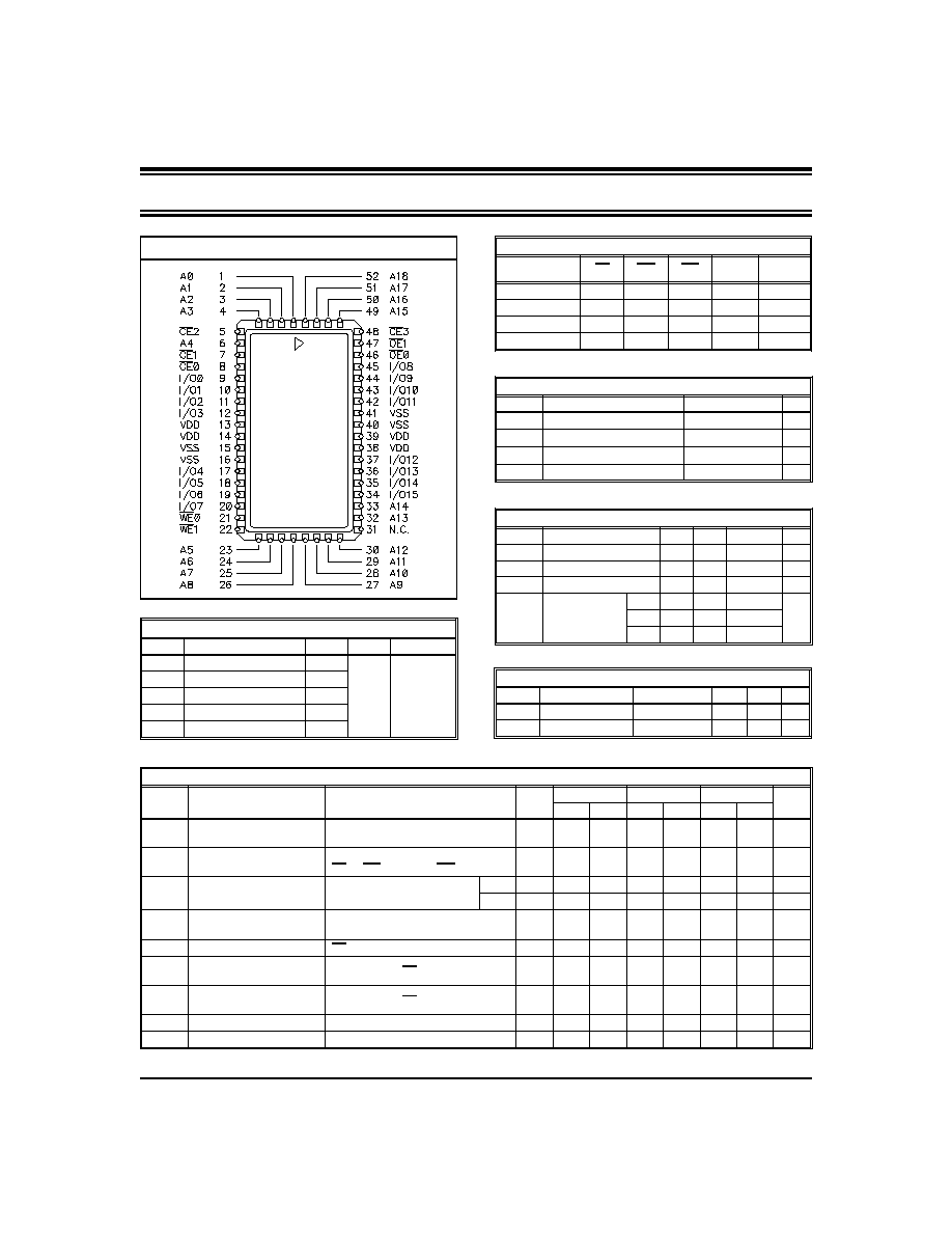
A0 - A18
Address Inputs
I/O0 - I/O15
Data Input/Output
CE0 - CE3
Low Chip Enables
WE0, WE1
Write Enables
OE0, OE1
Output Enables
V
DD
Power (+5V)
V
SS
Ground
N.C.
No Connect
2Mx16, 20 - 45ns, STACK
30A129-08
A
SLCC Stack
Straight
Leaded
Stack
Gullwing
Leaded
Stack
`'J'' Leaded
Stack
This document contains information on a product that is currently released
to production at Dense-Pac Microsystems, Inc. Dense-Pac reserves the
right to change products or specifications herein without prior notice.
30A129-08
REV. A
1
DPS2MX16MKn3
Dense-Pac Microsystems, Inc.
RECOMMENDED OPERATING RANGE
3
Symbol
Characteristic
Min. Typ.
Max.
Unit
V
DD
Supply Voltage
4.5
5.0
5.5
V
V
IH
Input HIGH Voltage 2.2
V
DD
+0.3 V
V
IL
Input LOW Voltage -0.5
2
0.8
V
T
A
Operating
Temperature
M/B -55 +25
+125
o
C
I
-40 +25
+85
C
0
+25
+70
TRUTH TABLE
Mode
CE
WE
OE
I/O Pin Supply
Current
Not Selected
H
X
X
High-Z Standby
D
OUT
Disable
L
H
H
High-Z Active
Read
L
H
L
D
OUT
Active
Write
L
L
X
D
IN
Active
H = HIGH L = LOW X = Don't Care
DC OPERATING CHARACTERISTICS: Over operating ranges
Symbol
Characteristics
Test Conditions
Typ.
()
C
I
M/B
Unit
Min.
Max.
Min.
Max.
Min.
Max.
I
IN
Input
Leakage Current
V
IN
= 0V to V
DD
-
-40
+40
-40
+40
-40
+40
µ
A
I
OUT
Output
Leakage Current
V
I/O
= 0V to V
DD
,
CE or OE = V
IH
, or WE = V
IL
-
-40
+40
-40
+40
-40
+40
µ
A
I
CC
Operating
Supply Current
Cycle=min., Duty=100%
I
OUT
= 0mA
x8
265
590
600
600
mA
x16
370
700
720
720
I
SB1
Full Standby
Supply Current
V
IN
V
DD
-0.2V or
V
IN
V
SS
+0.2V
8
80
80
120
mA
I
SB2
Standby Current (TTL)
CE = V
IH
160
480
480
480
mA
I
DR3
Data Retention
Supply Current (3.0V)
V
DR
= 3.0V, CE
V
DR
-0.2V
1.2
4.0
8.0
16.0
mA
I
DR2
Data Retention
Supply Current (2.0V)
V
DR
= 2.0V, CE
V
DR
-0.2V
0.8
2.4
6.4
14.4
mA
V
OL
Output Low Voltage
I
OUT
= 8.0mA
-
0.4
0.4
0.4
V
V
OH
Output High Voltage
I
OUT
= -4.0mA
-
2.4
2.4
2.4
V
Typical measurements made at +25
o
C, Cycle = min., V
DD
= 5.0V.
CAPACITANCE
4
: T
A
= 25
°
C, F = 1.0MHz
Symbol
Parameter
Max.
Unit
Condition
C
ADR
Address Input
80
pF
V
IN
2
= 0V
C
CE
Chip Enable
32
C
WE
Write Enable
40
C
OE
Output Enable
40
C
I/O
Data Input/Output
50
PIN-OUT DIAGRAM
DC OUTPUT CHARACTERISTICS
Symbol
Parameter
Conditions
Min. Max. Unit
V
OH
HIGH Voltage
I
OH
= -4.0mA 2.4
V
V
OL
LOW Voltage
I
OL
=8.0mA
0.4
V
ABSOLUTE MAXIMUM RATINGS
3
Symbol
Parameter
Value
Unit
T
STC
Storage Temperature
-65 to +150
°
C
T
BIAS
Temperature Under Bias
-55 to +125
°
C
V
DD
Supply Voltage
1
-0.5 to +7.0
°
C
V
I/O
Input/Output Voltage
1
-0.5 to V
DD
+0.5
V
30A129-08
REV. A
2
Dense-Pac Microsystems, Inc.
DPS2MX16MKn3
+5V
255
480
C
L
*
D
OUT
Figure 1. Output Load
* Including Probe and Jig Capacitance.
OUTPUT LOAD
Load
C
L
Parameters Measured
1
100pF
except t
LZ
, t
HZ
, t
OHZ
, t
OLZ
, and t
WHZ
2
5pF
t
LZ
, t
HZ
, t
OHZ
, t
OLZ
, and t
WHZ
AC TEST CONDITIONS
Input Pulse Levels
0V to 3.0V
Input Pulse Rise and Fall Times
5ns
Input and Output
Timing Reference Levels
1.5V
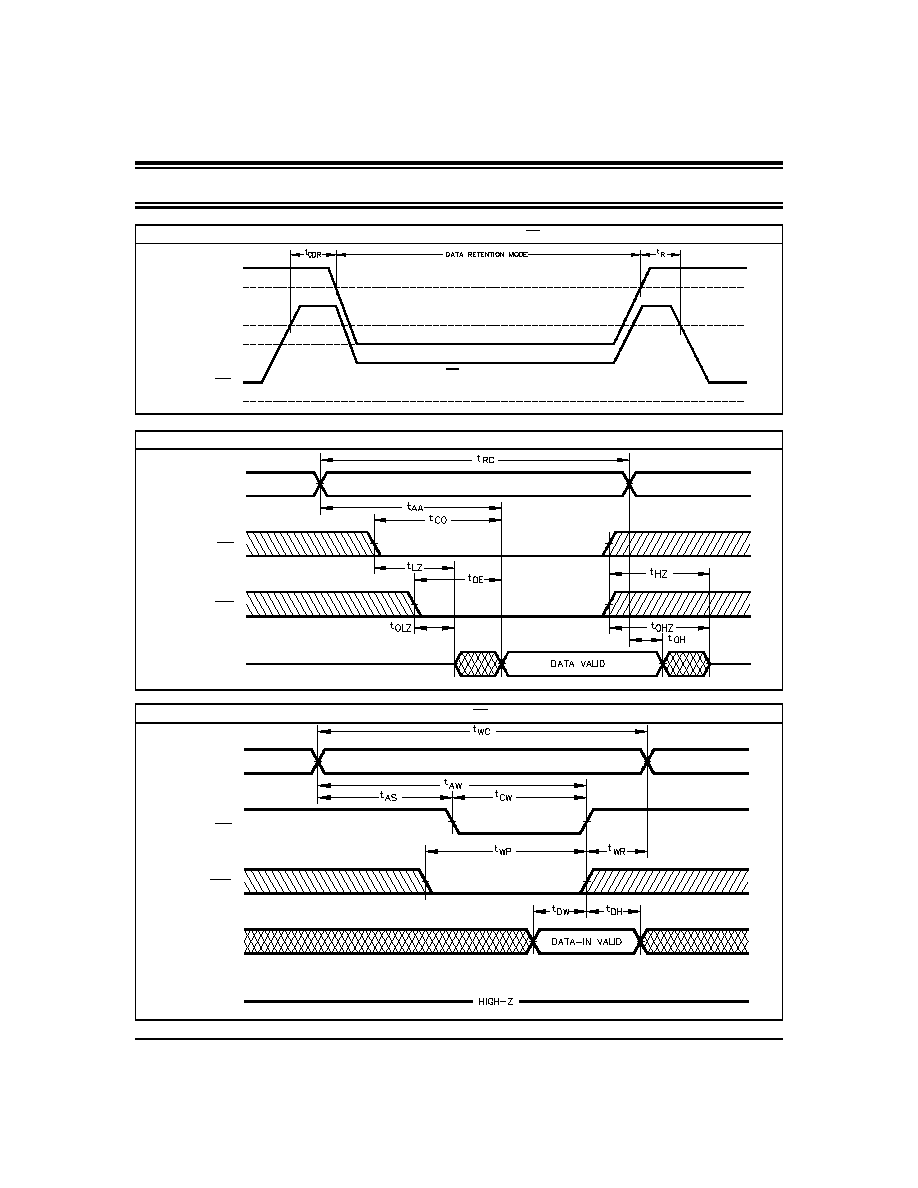
Data Retention AC Characteristics
8
Symbol
Parameter
Test Conditions
Min.
Typ.
Max.
Unit
V
DR
V
DD
for Data Retention
CE
V
DR
-0.2V
2.0
-
-
V
V
CDR
Chip Disable to
Data Retention Time
See Data Retention Waveform
0
-
-
ns
t
R
Operation Recovery Time
See Data Retention Waveform
5
-
-
ms
AC OPERATING CONDITIONS AND CHARACTERISTICS - READ CYCLE:
Over operating ranges
No. Symbol
Parameter
20ns*
25ns
30ns
35ns
45ns
Unit
Min.
Max.
Min.
Max.
Min. Max.
Min.
Max.
Min. Max.
1
t
RC
Read Cycle Time
20
25
30
35
45
ns
2
t
AA
Address Access Time
20
25
30
35
45
ns
3
t
CO
CE to Output Valid
20
25
30
35
45
ns
4
t
OE
Output Enable to Output Valid
10
12
15
20
25
ns
5
t
LZ
CE to Output in LOW-Z
4, 5
3
3
3
3
3
ns
6
t
OLZ
Output Enable to Output in LOW-Z
4, 5
0
0
0
0
0
ns
7
t
HZ
CE to Output in HIGH-Z
4, 5
8
10
15
20
25
ns
8
t
OHZ
Output Enable to Output in HIGH-Z
4, 5
0
8
0
10
0
15
0
20
0
25
ns
9
t
OH
Output Hold from Address Change
4
5
5
5
5
ns
AC OPERATING CONDITIONS AND CHARACTERISTICS - WRITE CYCLE
6, 7
:
Over operating ranges
No. Symbol
Parameter
20ns*
25ns
30ns
35ns
45ns
Unit
Min.
Max.
Min.
Max.
Min. Max.
Min.
Max.
Min. Max.
10
t
WC
Write Cycle Time
20
25
30
35
45
ns
11
t
AW
Address Valid to End of Write
13
15
20
25
35
ns
12
t
CW
Chip Enable to End of Write
13
15
20
25
35
ns
13
t
AS
Address Set-Up Time **
0
0
0
0
0
ns
14
t
WP
Write Pulse Width
13
15
20
25
35
ns
15
t
WR
Write Recovery Time
0
0
0
0
0
ns
16
t
WHZ
Write Enable to Output in HIGH-Z
4, 5
0
8
0
10
0
12
0
15
0
20
ns
17
t
DW
Data to Write Time Overlap
9
10
12
15
20
ns
18
t
DH
Data Hold from Write Time
0
0
0
0
0
ns
19
t
OW
Output Active from End of Write
3
3
3
3
3
ns
* Available in Commercial and Industrial Grade Only.
** Valid for both Read and Write Cycles.
30A129-08
REV. A
3
DPS2MX16MKn3
Dense-Pac Microsystems, Inc.
READ CYCLE
ADDRESS
CE
OE
DATA I/O
DATA RETENTION WAVEFORM:
CE Controlled.
V
DD
4.5V
2.3V
V
DR1
CE
0V
CE
V
DD
-0.2V
WRITE CYCLE 1:
CE Controlled.
ADDRESS
CE
WE
DATA IN
DATA OUT
30A129-08
REV. A
4
Dense-Pac Microsystems, Inc.
DPS2MX16MKn3
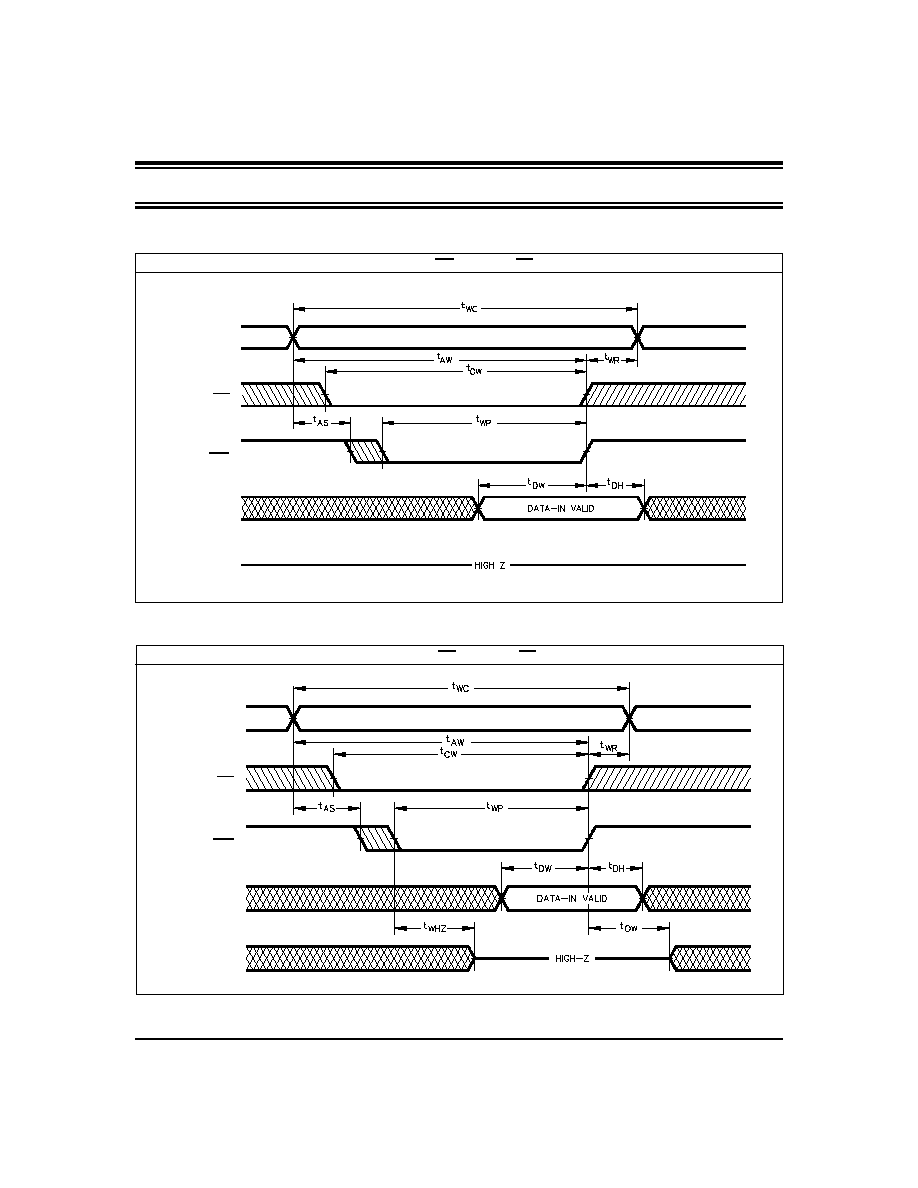
WRITE CYCLE 2:
WE Controlled. OE is HIGH.
8
ADDRESS
CE
WE
DATA IN
DATA OUT
WRITE CYCLE 3:
WE Controlled. OE is LOW.
8
ADDRESS
CE
WE
DATA IN
DATA OUT
30A129-08
REV. A
5
DPS2MX16MKn3
Dense-Pac Microsystems, Inc.
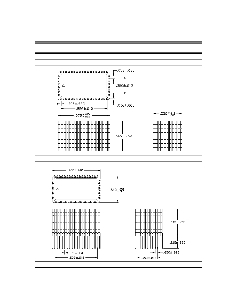
(52 - PIN LEADLESS STACK) MECHANICAL DRAWING
(52 - PIN STRAIGHT LEADED STACK) MECHANICAL DRAWING
30A129-08
REV. A
6
Dense-Pac Microsystems, Inc.
DPS2MX16MKn3
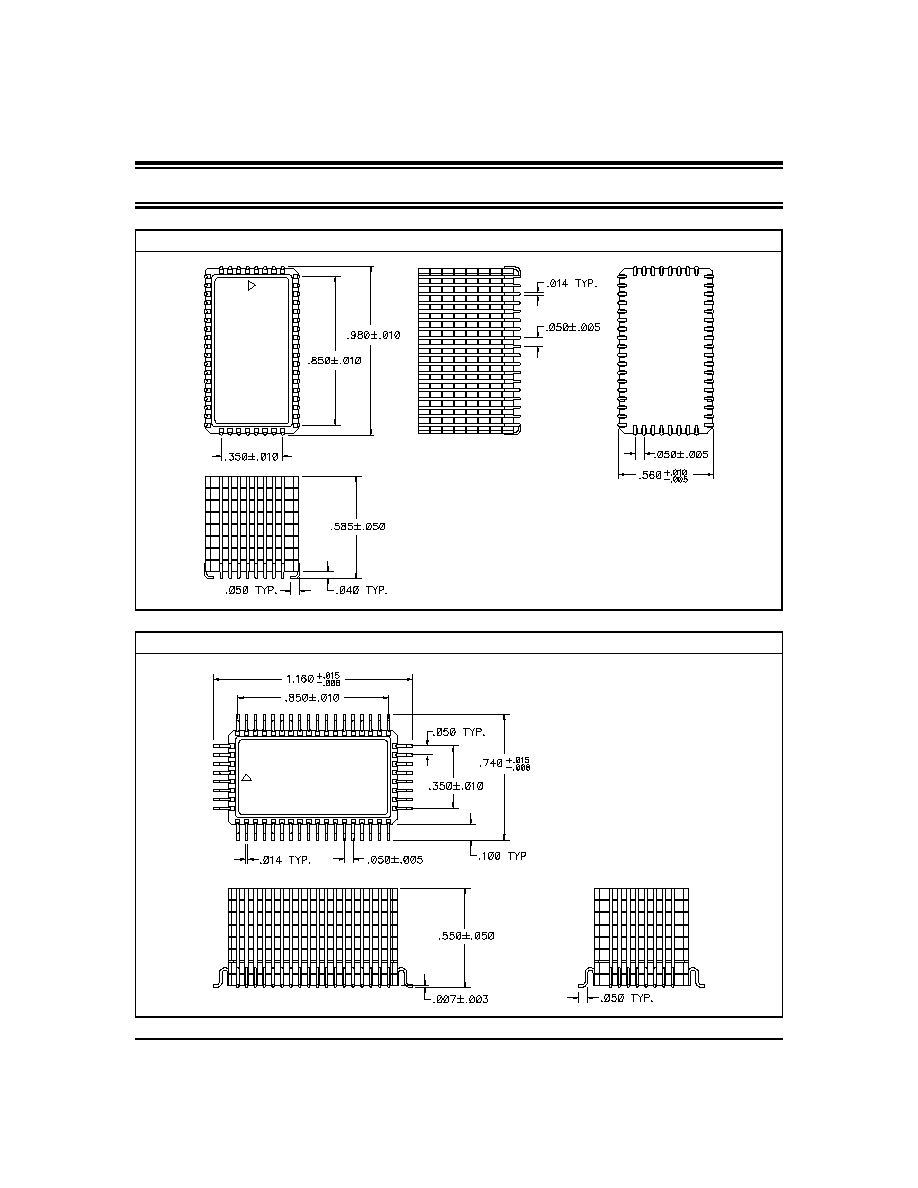
(52 - PIN `'J'' LEADED STACK) MECHANICAL DRAWING
(52 - PIN GULLWING LEADED STACK) MECHANICAL DRAWING
30A129-08
REV. A
7
DPS2MX16MKn3
Dense-Pac Microsystems, Inc.
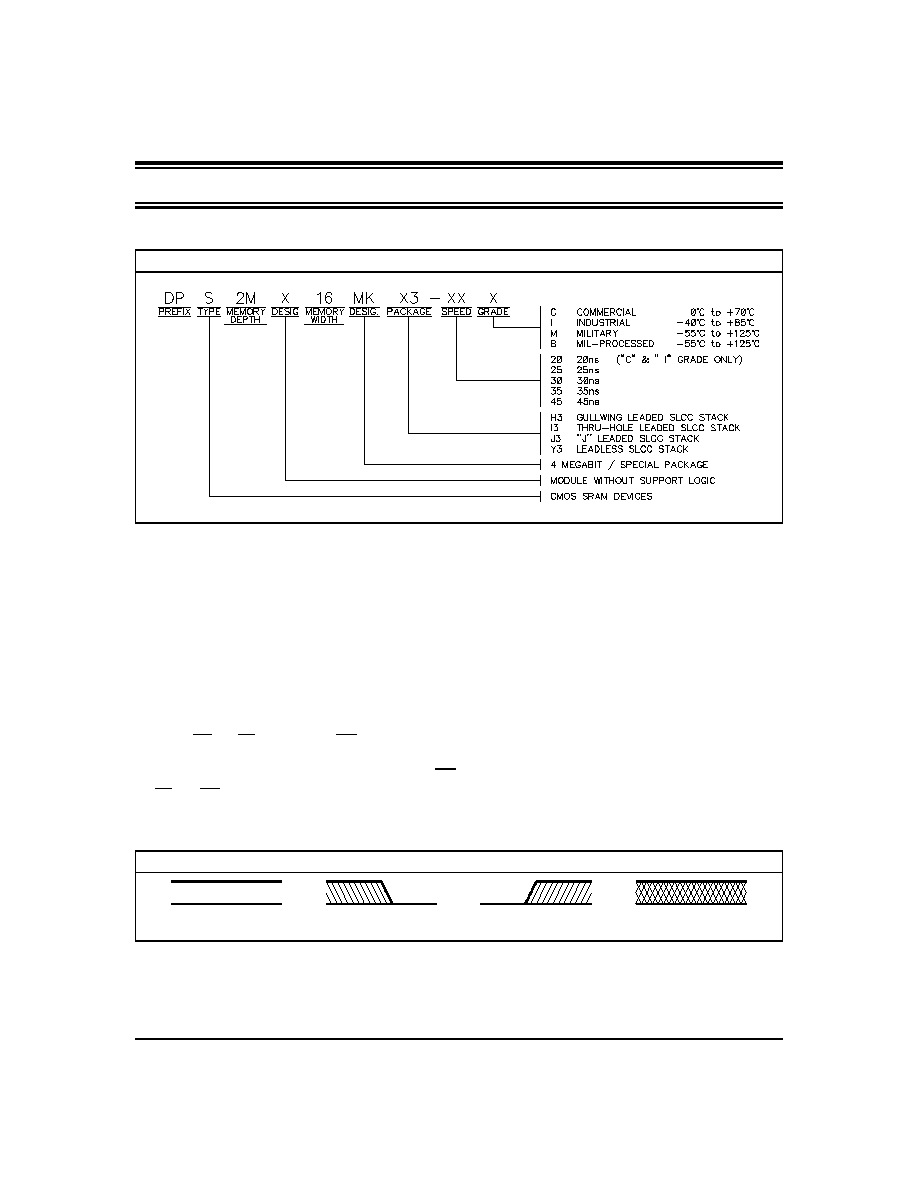
ORDERING INFORMATION
Dense-Pac Microsystems, Inc.
7321 Lincoln Way ¿ Garden Grove , California 92841-1431
(714) 898-0007 (800) 642-4477
(Outside CA)
¿ FAX: (714) 897-1772 ¿ http://www.dense-pac.com
WAVEFORM KEY
Data Valid
Transition from
Transition from
Data Undefined
HIGH to LOW
LOW to HIGH
or Don't Care
NOTES:
1. All voltages are with respect to V
SS
.
2. -2.0V min. for pulse width less than 20ns (V
IL
min. = -0.5V at DC level).
3. Stresses greater than those under
ABSOLUTE MAXIMUM RATINGS may cause permanent damage to the device.
This is a stress rating only and functional operation of the device at these or any other conditions above those
indicated in the operational sections of this specification is not implied. Exposure to absolute maximum rating
conditions for extended periods may affect reliability.
4. This parameter is guaranteed and not 100% tested.
5. Transition is measured at the point of
±
500mV from steady state voltage.
6. When OE and CE are LOW and WE is HIGH, I/O pins are in the output state,and input signals of opposite phase
to the outputs must not be applied.
7. The outputs are in a high impedance state when WE is LOW.
8. CE and WE can initiate and terminate WRITE Cycle.
30A129-08
REV. A
8