30A248-00
REV. B 12/02
This document contains information on a product that is currently released to production at DPAC Technologies.
DPAC reserves the right to change products or specifications herein without prior notice.
1 Gigabit Synchronous DRAM
DPSD128MX8XKY5
1
ADVAN C E D C O M P O N E NTS PAC K AG I N G
DESCRIPTION:
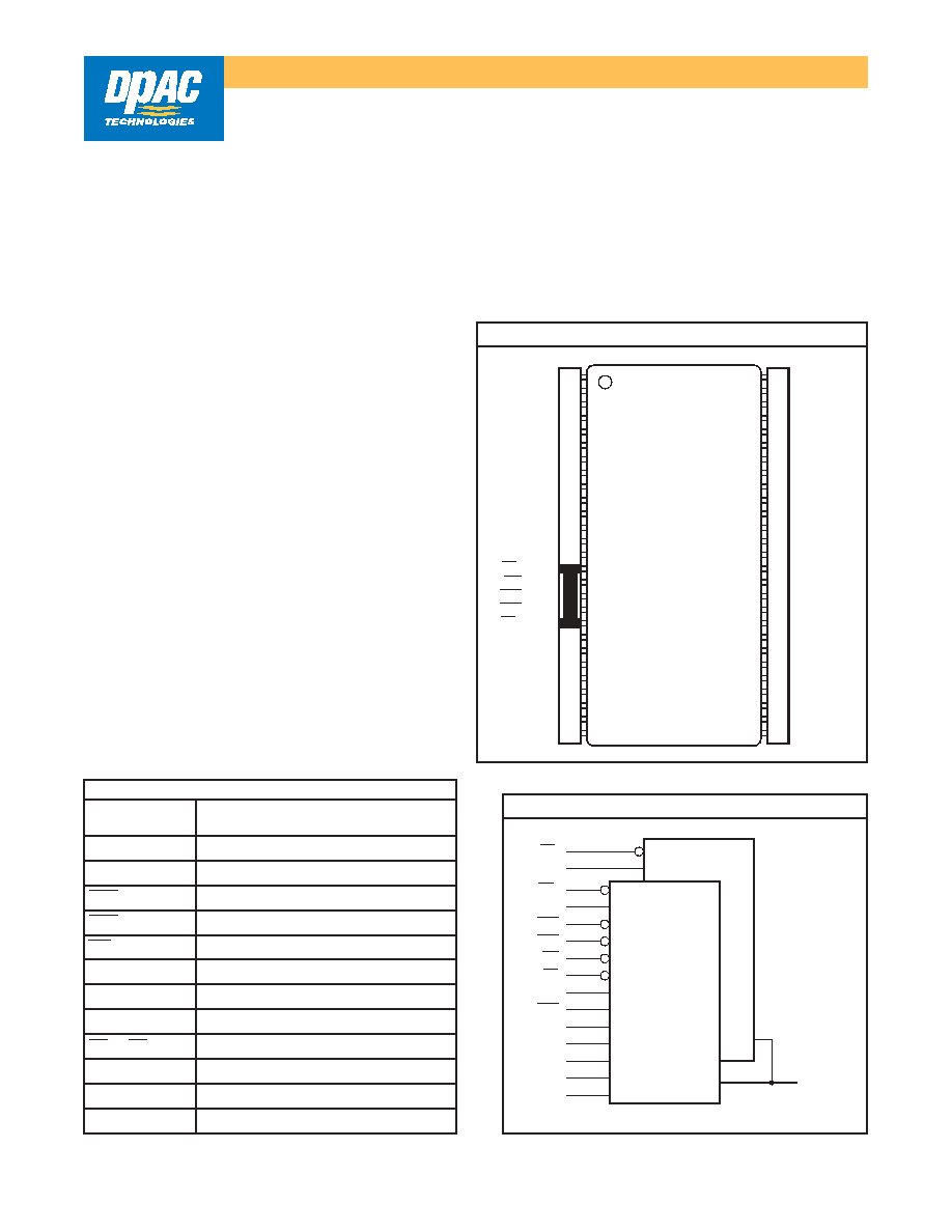
The Memory StackTM series is a family of interchangeable memory modules. The 1 Gigabit SDRAM is a member of this
family which utilizes the space saving LP-StackTM TSOP stacking technology. The modules are constructed with two 64 Meg
x 8 SDRAMs.
This 1 Gigabit LP-StackTM module, DPSD128MX8XKY5, has been designed to fit the same footprint as the 64 Meg x 8
SDRAM TSOP monolithics and 512 Megabit based family of LP-Stack.TM modules. This allows system upgrade without
electrical or mechanical redesign, providing an immediate and low cost memory solution.
FEATURES:
∑ Configuration: 128 Meg x 8 bit
(2 Banks x 16M x 4 Bit x 8 Banks)
∑ JEDEC Approved Footprint and Pinout
∑ IPC-A-610 Manufacturing Standards
∑ Assemble per DPAC Application Note 53A001-00
∑ Package: 54-Pin LP-StackTM
The Following Features are not affected by LP StackTM and
are provided as reference only. Refer to memory OEM
Device specification for details:
∑ Clock Frequency is determined by OEM memory
device used.
∑ 3.3 Volt DQ Supply
∑ LVTTL Compatible I/O
∑ Four Bank Operation
∑ Programmable Burst Type, Burst Length, and CAS
Latency
∑ Refresh: 8192 Cycles / 64ms
∑ Refresh Types: Auto and Self
FUNCTIONAL BLOCK DIAGRAM
DM
CAS
WE
DQ0-DQ7
CS0
(8 Meg x 8 Bits x 4 Banks)
RAS
CK
DQS
CS1
CK
A0-A12
VREF
CKE1
CKE0
(8 Meg x 6 Bits x 4 Banks)
BA0-BA1
256 Mb DDR SDRAM
QFC
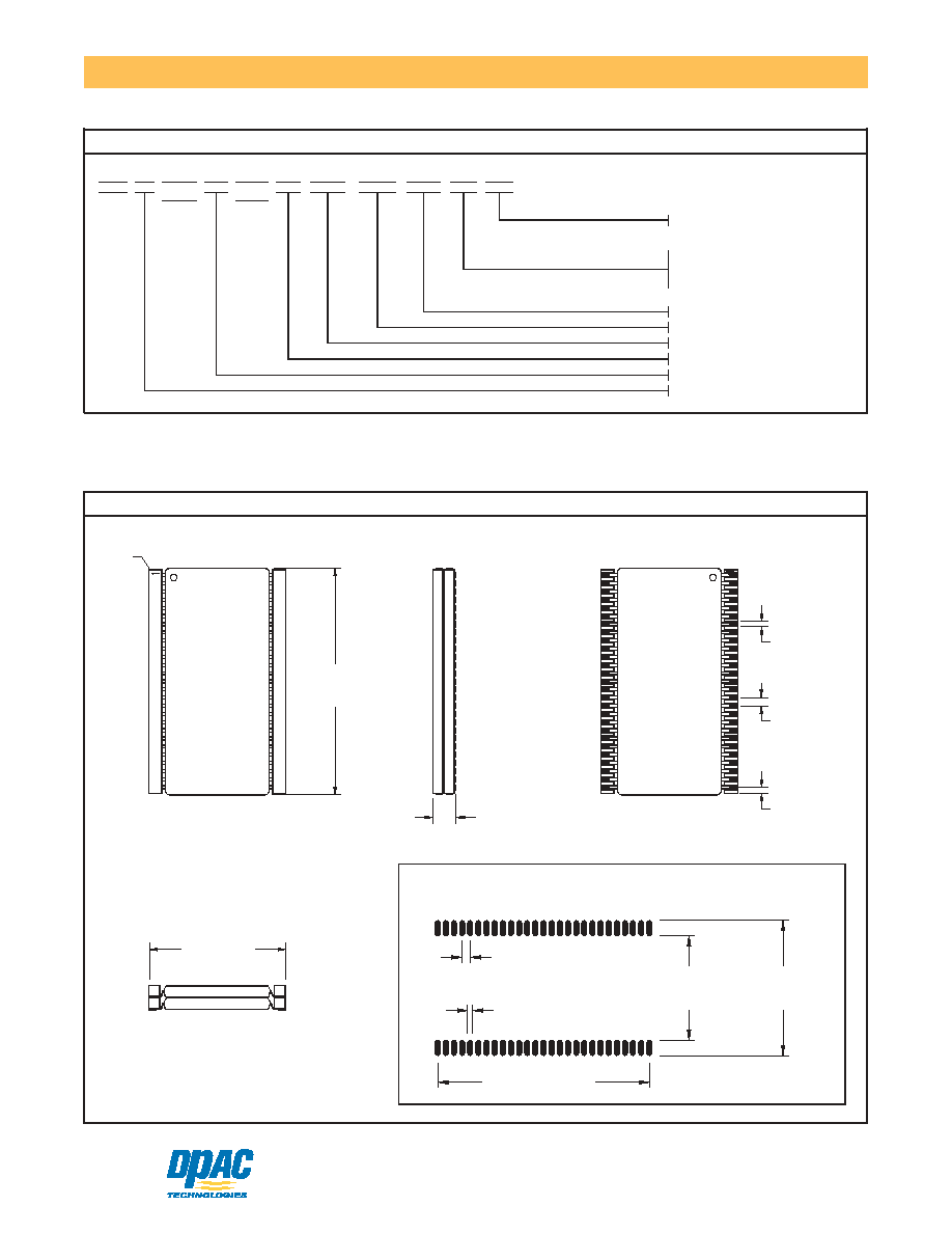
PINOUT DIAGRAM
(TOP VIEW)
33
A8
VCC
1
DQ0
2
54
VSS
VCCQ
3
53
DQ7
N.C.
4
52
VSSQ
DQ1
5
51
N.C.
VSSQ
6
50
DQ6
N.C.
7
49
VCCQ
DQ2
8
48
N.C.
VCCQ
9
47
DQ5
N.C.
10
46
VSSQ
DQ3
11
45
N.C.
VSSQ
12
44
DQ4
N.C.
13
43
VCCQ
VCC
14
42
N.C.
CS1
15
41
VSS
WE
16
40
N.C.
CAS
17
39
DQM
RAS
18
38
CLK
CS0
19
37
CKE
BA0
20
36
A12
BA1
21
35
A11
A10
22
34
A9
A0
23
32
A7
A1
24
31
A6
A2
25
30
A5
A3
26
29
A4
VCC
27
28
VSS
1
PIN NAMES
A0-A12
Row Address:
RA0-RA12
Column Address:
CA0-CA9, A11, A12
BA0, BA1
Bank Select Address
DQ0-DQ7
Data In/Data Out
CAS
Column Address Strobe
RAS
Row Address Strobe
WE
Data Write Enable
DQM
Data Input/Output Mask
CKE
Clock Enables
CLK
System Clock
CS0 - CS1
Chip Selects
V
DD/
V
SS
Power Supply/Ground
V
DDQ/
V
SSQ
Data Output Power/Ground
N.C.
No Connect
30A248-00
REV. B 12/02
2
DPAC Technologies Products & Services for the Integration Age
7321 Lincoln Way, Garden Grove, CA 92841 Tel 714 898 0007 Fax 714 897 1772
www.dpactech.com Nasdaq: DPAC
©2002 DPAC Technologies, all rights reserved. DPAC TechnologiesTM, Memory StackTM, System StackTM, LP-StackTM, CS-StackTM are trademarks of DPAC Technologies Corp.
DPSD128MX8XKY5
1 Gigabit Synchronous DRAM
NOTE: [1] Contact your sales representative for supplier and manufacturer codes.
ORDERING INFORMATION
MANUFACTURER CODE
P12
DP
XX
XXX
-
SPEED
MEMORY
PREFIX
PC100 CAS LATENCY 2
SD 128M
X
8
Y5
PACKAGE
MEMORY
DESIG
MEMORY
TYPE
MEMORY MODULE WITHOUT SUPPORT LOGIC
DEPTH
WIDTH
DESIG
XK
STACKABLE TSOP
SYNCHRONOUS DRAM
SUPPLIER
- DP
SUPPLIER CODE
512 MEGABIT LVTTL BASED
GRADE
X
Commercial Temperature
Blank
[1]
[1]
75
7.5ns (133MHz)
PC100 CAS LATENCY 3
P13
MECHANICAL DIAGRAM
.020 [.51]
.0315 [.80]
.0305 [.775]
TOP VIEW
SIDE VIEW
BOTTOM VIEW
END VIEW
PIN 1
INDEX
.502±.008
.102 MAX.
.885±.010
.407 [10.34]
.397 [10.08]
.527 [13.39]
.517 [13.13]
.0315 [.80] BSC
.018 [.46]
RECOMMENDED PAD LAYOUT
[12.75±.20]
[22.48±.25]
[2.59 MAX.]
.819 [20.80] BSC
.022 [.56]
Dimensions - Inches [mm]