768 Megabit Synchronous DRAM
DPSD96MX8WKY5
DESCRIPTION:
The LP-StackTM series is a family of interchangeable memory modules. The 768 Megabit SDRAM is a member of this family which utilizes the new
and innovative space saving TSOP stacking technology. The modules are constructed with 32 Meg x 8 SDRAMs.
This 256 Megabit based LP-StackTM module, the DPSD96MX8WKY5 has
been designed to fit in the same footprint as the 32 Meg x 8 SDRAM TSOP
monolithic and 256 Megabit SDRAM based family of LP-StackTM modules.
This allows the memory board designer to upgrade the memory in their
products without redesigning the memory board, thus saving time and
money.
FEATURES:
·
Configuration Available:
96 Meg x 8 (3 Banks of 8M x 4 x 8 bits)
·
Clock Frequency:
66
[1]
, 83
[1]
, 100, 125
[2]
, 133
[2]
MHz (max.)
·
PC100 and PC133 Compatible
·
3.3V Supply
·
LVTTL Compatible I/O
·
Four Bank Operation
·
Programmable Burst Type, Burst Length,
and CAS Latency
·
8192 Cycles / 64 ms
·
Auto and Self Refresh
·
Package: TSOP Leadless Stack
NOTES:
[1] Available in Industrial Temperature Ranges Only
[2] Available in Commercial Temperature Range Only.
ADVANCED
INFORMATION
1
30A226-30
REV. A
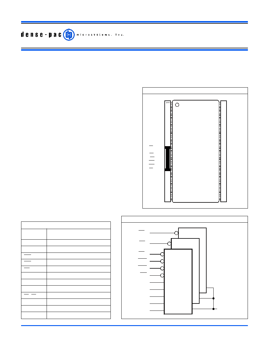
PIN-OUT DIAGRAM
(TOP VIEW)
33
A8
VCC
1
DQ0
2
54
VSS
VCCQ
3
53
DQ7
N.C.
4
52
VSSQ
DQ1
5
51
N.C.
VSSQ
6
50
DQ6
N.C.
7
49
VCCQ
DQ2
8
48
N.C.
VCCQ
9
47
DQ5
N.C.
10
46
VSSQ
DQ3
11
45
N.C.
VSSQ
12
44
DQ4
CS2
13
43
VCCQ
VCC
14
42
N.C.
CS1
15
41
VSS
WE
16
40
N.C.
CAS
17
39
DQM
RAS
18
38
CLK
CS0
19
37
CKE
BA0
20
36
A12
BA1
21
35
A11
A10
22
34
A9
A0
23
32
A7
A1
24
31
A6
A2
25
30
A5
A3
26
29
A4
VCC
27
28
VSS
PIN NAMES
A0 - A12
Row Address:
A0 - A12
Column Address: A0 - A9, A11
BA0, BA1
Bank Select Address
DQ0 - DQ7
Data In / Data Out
CAS
Column Address Strobes
RAS
Row Address Enables
WE
Data Write Enable
DQM
Data Input/Output Mask
CKE
Clock Enable
CLK
System Clock
CS0-CS2
Chip Selects
V
CC
/V
SS
Power Supply/Ground
V
CCQ
/V
SSQ
Data Output Power/Ground
N.C.
No Connect
FUNCTIONAL BLOCK DIAGRAM
A0-A12
CAS
WE
256
Mbit
SDRAM
DQ0-DQ7
CS0
(4x8Mx8bit)
(4x8Mx8bit)
RAS
CKE
CLK
CS1
DQM
BA0,BA1
CS2
(4x8Mx8bit)
This document contains information on a product presently under development at Dense-Pac Microsystems, Inc.
Dense-Pac reserves the right to change products or specifications herein without prior notice.
DPSD96MX8WKY5
Dense-Pac Microsystems, Inc.
NOTES:
[1] Available in Industrial Temperature Ranges Only, see note 4.
[3] Contact your sales representative for supplier and manufacturer codes.
[2] Available in Commercial Temperature Range Only.
[4] All industrial temperature range parts are subject to availability of screened components.
ADVANCED
INFORMATION
PART NUMBERING DESCRIPTION
2
30A226-30
REV. A
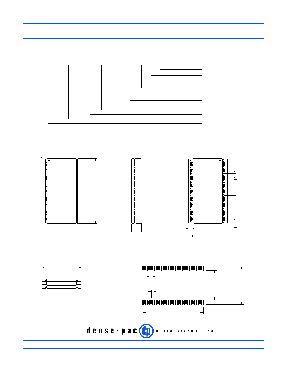
MECHANICAL DRAWING
.020 [.51]
.0315 [.80]
.0305 [.775]
TOP VIEW
SIDE VIEW
BOTTOM VIEW
END VIEW
PIN 1
INDEX
.502±.008
.150 MAX.
.0335 [.85]
.885±.010
.407 [10.34]
.397 [10.08]
.527 [13.39]
.517 [13.13]
.0315 [.80] BSC
.018 [.46]
Standard TSOP pad layout is acceptable, however, when possible,
the following pad layout is recommended for optimal manufacture and
inspection. See Application Note 53A001-00 for further information.
[12.75±.20]
[22.48±.25]
[3.81 MAX.]
.819 [20.80] BSC
.022 [.56]
[11.76±.20]
.463±.008
MANUFACTURER CODE
P1
DP
XX
XX
-
SPEED
MEMORY
PREFIX
PC100
SD 96M
X
8
Y5
PACKAGE
MEMORY
DESIG
MEMORY
TYPE
MEMORY MODULE WITHOUT SUPPORT LOGIC
DEPTH
WIDTH
DESIG
WK
STACKABLE TSOP
SYNCHRONOUS DRAM
10ns (100MHz)
8ns (125MHz)
08
10
SUPPLIER
- DP
SUPPLIER CODE
256 MEGABIT LVTTL BASED
15
12
12ns (83MHz)
15ns (66MHz)
CL
X
GRADE
X
CAS LATENCY 2
2
I
Industrial Temperature
Commercial Temperature
Blank
[1]
[1]
[2]
[3]
[3]
[2]
[1]
[1]
[2]
[2]
75
7.5ns (133MHz)
[4]
[4]
7321 lincoln way, garden grove, california 92841-1431
·
(714) 898-0007
·
(800) 642-4477
·
fax: (714) 897-1772
·
http://www.dense-pac.com