4 Megabit FLASH EEPROM
DPZ256X16In3
DESCRIPTION:
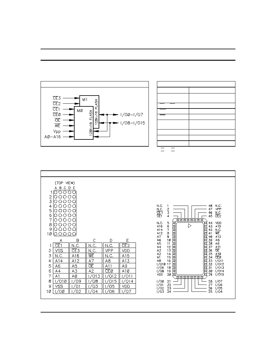
The DPZ256X16In3 `'STACK'' modules are a revolutionary new
memory subsystem using Dense-Pac Microsystems' ceramic
Stackable Leadless Chip Carriers (SLCC). Available in straight
leaded, `'J'' leaded or gullwing leaded packages, or mounted on a
50-pin PGA co-fired ceramic substrate. The module packs
4-Megabits of FLASH EEPROM in an area as small as 0.463 in
2
,
while maintaining a total height as low as 0.171 inches.
The DPZ256X16In3 STACK modules contain two individual SLCC
packages each containing two 128K x 8 FLASH memory devices.
Each SLCC is hermetically sealed making the module suitable for
commercial, industrial and military applications.
By using SLCCs, the `'Stack'' family of modules offer a higher board
density of memory than available with conventional through-hole,
surface mount or hybrid techniques.
FEATURES:
∑
Organization:
256K x 16 or 512K x 8
∑
Fast Access Times (max.):
120, 150, 170, 200, 250ns
∑
Fully Static Operation - No clock or refresh required
∑
TTL Compatible Inputs and Outputs
∑
Common Data Inputs and Outputs
∑
10,000 Erase/Program Cycles (min.)
∑
Packages Available:
48 - Pin SLCC Stack
48 - Pin Straight Leaded Stack
48 - Pin `'J'' Leaded Stack
48 - Pin Gullwing Leaded Stack
50 - Pin PGA Dense-Stack
DPZ256X16IH3
DPZ256X16IJ3
DPZ256X16IA3
DPZ256X16IY3
DPZ256X16II3
This document contains information on a product that is currently released
to production at Dense-Pac Microsystems, Inc. Dense-Pac reserves the
right to change products or specifications herein without prior notice.
30A071-12
REV. E
1

Dense-Pac Microsystems, Inc.
DPZ256X16In3
DEVICE OPERATION:
The FLASH devices are electrically erasable and
programmable memories that function similarly to an EPROM
device, but can be erased without being removed from the
system and exposed to ultraviolet light. Each 128K x 8 device
can be erased individually eliminating the need to re-program
the entire module when partial code changes are required.
READ:
With V
PP
= 0V to V
DD
(V
PPLO
)
, the devices are read-only
memories and can be read like a standard EPROM. By
selecting the device to be read (see Truth Table and
Functional Block Diagram)
, the data programmed into the
device will appear on the appropriate I/O pins.
When V
PP
= +12.0V
±
0.6V (V
PPHI
)
, reads can be
accomplished in the same manner as described above but
must be preceded by writing 00H
1
to the command register
prior to reading the device. When V
PP
is raised to V
PPHI
the
contents of the command register default to 00H
1
and remain
that way until the command register is altered.
STANDBY:
When the appropriate CE`s are raised to a logic-high level, the
standby operation disables the FLASH devices reducing the
power consumption substantially. The outputs are placed in
a high- impedance state, independent of the OE input. If the
module is deselected during programming or erase, the
device upon which the operation was being performed will
continue to draw active current until the operation is
completed.
PROGRAM:
The programming and erasing functions are accessed via the
command register when high voltage is applied to V
PP
. The
contents of the command register control the functions of the
memory device (see Command Definition Table).
The command register is not an addressable memory
location. The register stores the address, data, and command
information required to execute the command. When V
PP
=
V
PPLO
the command register is reset to 00H
1
returning the
device to the read-only mode.
The command register is written by enabling the device upon
which that the operation is to be performed (see Functional
Block Diagram)
. While the device is enabled bring WE to a
logic-low (V
IL
). The address is latched on the falling edge of
WE and data is latched on the rising edge of WE.
Programming is initiated by writing 40H
1
(program setup
command)
to the command register. On the next falling edge
of WE the address to be programmed will be latched,
followed by the data being latched on the rising edge of WE
(see AC Operating and Characteristics Table)
.
PROGRAM VERIFY:
The FLASH devices are programmed one location at a time.
Each location may be programmed sequentially or at random.
Following each programming operation, the data written
must be verified.
To initiate the program-verify mode, C0H
1
must be written to
the command register of the device just programmed. The
programming operation is terminated on the rising edge of
WE. The program-verify command is then written to the
command register.
After the program-verify command is written to the command
register, the memory device applies an internally generated
margin voltage to the location just written. After waiting 6
µ
s
the data written can be verified by doing a read. If true data
is read from the device, the location write was successful and
the next location may be programmed.
If the device fails to verify, the program/verify operation is
repeated up to 25 times.
ERASE:
The erase function is a command-only operation and can only
be executed while V
PP
= V
PPHI
.
To setup the chip-erase, 20H
1
must be written to the
command register. The chip-erase is then executed by once
again writing 20H
1
to the command register (see AC
Operating and Characteristics Table)
.
To ensure a reliable erasure, all bits in the device to be erased
should be programmed to their charged state (data = 00H)
prior to starting the erase operation. With the algorithm
provided, this operation should typically take 2 seconds.
HIGH PERFORMANCE PARALLEL ERASURE:
Dense-Pac recommends that all users implement the
following Intel High Performance Parallel Erase algorithm
in order to avoid the possibility of over erasing these parts.
In applications containing more than one FLASH memory,
you can erase each device serially or you can reduce total
erase time by implementing a parallel erase algorithm. You
may save time by erasing all devices at the same time.
However, since FLASH memories may erase at different rates,
you must verify each device separately. This can be done in
a word-wise fashion with the Command Register Reset
Command and a special masking algorithm.
Take for example the case of two-device (parallel) erasure.
The CPU first writes the data word erase command 2020H
twice in succession. This starts erasure. After 10ms, the CPU
writes the data word verify command A0A0H to stop erasure
and setup erase verification. If both one or both bytes are not
erased at the given address, the CPU implements the erase
sequence again without incrementing the address.
Suppose at the given address only the low byte verifies FFH
data? Could the whole chip be erased? The answer is yes.
Rather than check the rest of the low byte addresses
independently of the high byte, simply use the reset
command to mask the low byte from erasure and erase
verification on the next erase loop. In this example the erase
command would be 20FFH and the verify command would
be A0FFH. Once the high byte verifies at the address, the
CPU modifies the command back to the default 2020H and
A0A0H, increments to the next address, and then writes the
verify command.
See Figure 4 for a conceptual view of the parallel erase flow
chart and Figure 4 for the detailed version. These flow charts
are for the 16-bit systems and can be expanded for 32-bit
designs.
ERASE VERIFY:
The erase operation erases all locations in the device selected
in parallel. Upon completion of the erase operation, each
location must be verified. This operation is initiated by writing
A0H
1
to the command register. The address to be verified
must be supplied in order to be latched on the falling edge of
WE.
The memory device internally generates a margin voltage and
applies it to the addressed location. If FFH is read from the
30A071-12
REV. E
3

DPZ256X16In3
Dense-Pac Microsystems, Inc.
device, it indicates the location is erased. The erase/verify
command is issued prior to each location verification to latch
the address of the location to be verified. This continues until
FFH is not read from the device or the last address for the
device being erased is read.
If FFH is not read from the location being verified, an
additional erase operation is performed. Verification then
resumes from the last location verified. Once all locations in
the device being erased are verified, the erase operation is
complete. The verify operation should now be terminated by
writing a valid command such as program set-up to the
command register.
PRODUCT I.D. OPERATION:
The product I.D. operation outputs the manufacturer code
(89H) and the device code (B4H). This allows programming
equipment to match the device with the proper erase and
programming algorithms.
With CE and OE at a logic low level, raising A9 to V
ID
(see
DC Operating Characteristics)
will initiate the operation. The
manufacturer's code can then be read from address location
0000H and the device code can be read from address
location 0001H.
The I.D. codes can also be accessed via the command
register. Following a write of 90H to the command register,
a read from address location 0000H outputs the
manufacturer's code (89H). A read from address location
0001H outputs the device code (B4H). To terminate the
operation, it is necessary to write another valid command into
the register.
POWER UP/DOWN PROTECTION:
The FLASH devices are designed to protect against accidental
erasure or programming during power transitions. It makes
no difference as to which power supply, V
PP
or V
DD,
powers
up first. Power supply sequencing is not required. Internal
circuitry ensures that the command register is reset to the read
mode upon power up.
POWER SUPPLY DECOUPLING:
V
PP
traces should use trace widths and layout considerations
comparable to that of the V
DD
power bus. The V
PP
supply
traces should also be decoupled to help decrease voltage
spikes.
While the memory module has high-frequency,
low-inductance decoupling capacitors mounted on the
substrate connected to V
DD
and V
SS
, it is recommended that
a 4.7
µ
F to 10
µ
F electrolytic capacitor be placed near the
memory module connected across V
DD
and V
SS
for bulk
storage. Decoupling capacitors should also be placed near
the module, connected across V
PP
and V
SS
.
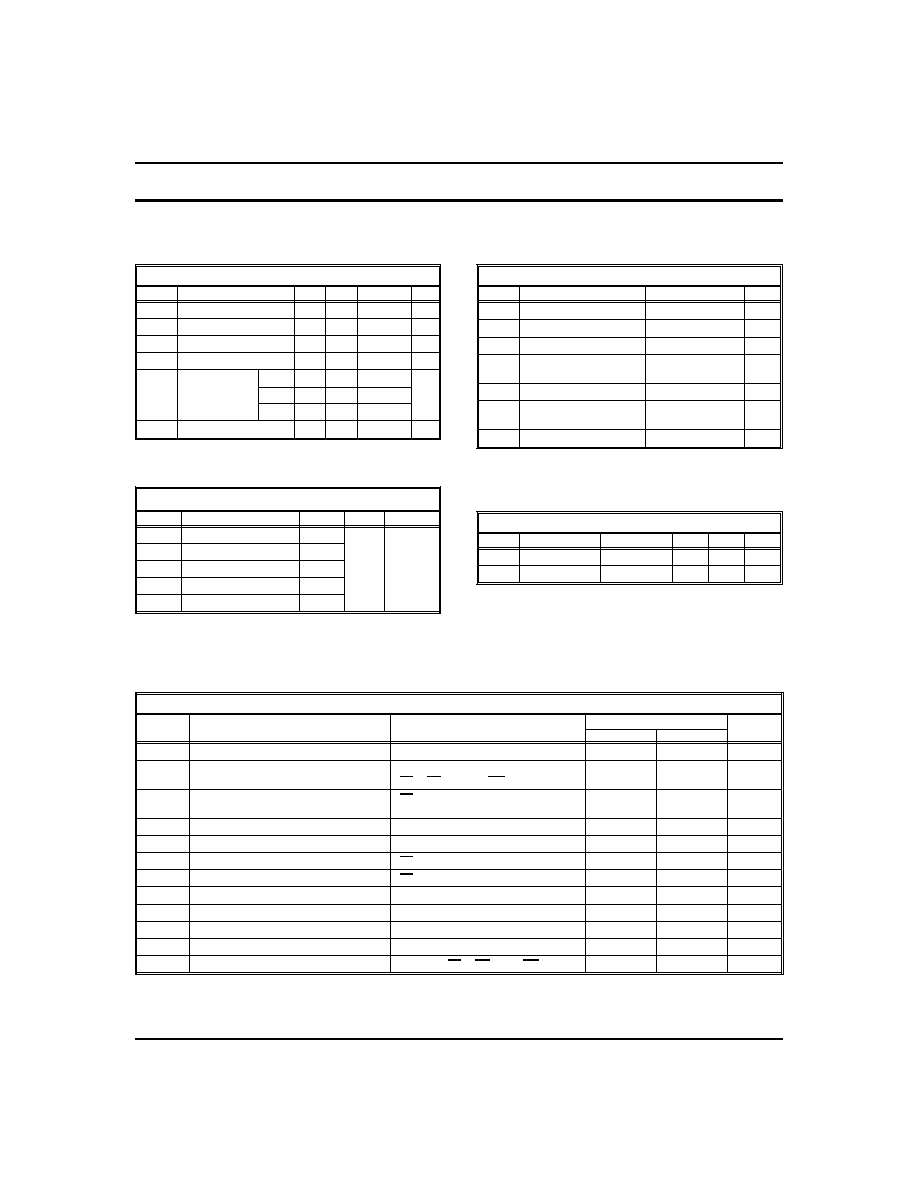
COMMAND DEFINITION TABLE
Command
Bus
Cycles
Req'd
First Bus Cycle
Second Bus Cycle
Operation
Address
Data
1
Operation
Address
Data
1
Read Memory
1
Write
X
00H
-
-
-
Setup Erase / Erase
2
Write
X
20H
Write
X
20H
Erase Verify
2
Write
EA
A0H
Read
X
EVD
Setup Program / Program
2
Write
X
40H
Write
PA
PD
Program Verify
2
Write
X
C0H
Read
X
PVD
Reset
2
Write
X
FFH
Write
X
FFH
Read Product I.D. Codes
3
Write
X
90H
Read
IA
ID
EA = Address to Verify
PA = Address to Program
EVD = Data Read from Location EA
PD = Data to be Programmed at Location PA
IA
= Address: 0000H for manufacturing code, 0001H for device code
PVA = Data to be Read from Location PA at Program Verify
ID = ID data read from IA during product ID operation
(Manufacturer = 89H, Device = B4H)
TRUTH TABLE
Mode
Description
CEn
WE
OE
A0
A9
V
PP
I/O Pins
Supply Current
READ
ONLY
Not Selected
H
X
X
X
X
V
PPLO
HIGH-Z
Standby
Output Disable
L
H
H
X
X
V
PPLO
HIGH-Z
Active
Read
L
H
L
A0
A9
V
PPLO
D
OUT
Active
I.D. (Mfr.)
L
H
L
L
V
ID
V
PPLO
D
OUT
=89H
Active
I.D. (Device)
L
H
L
H
V
ID
V
PPLO
D
OUT
= B4H
Active
COMMAND
PROGRAM
Not Selected
H
X
X
X
X
V
PPHI
HIGH-Z
Standby
Output Disable
L
H
H
X
X
V
PPHI
HIGH-Z
Active
Read
L
H
L
A0
A9
V
PPHI
D
OUT
Active
Write
L
L
H
A0
A9
V
PPHI
D
IN
Active
30A071-12
REV. E
4