DCR1277SD
1/9
APPLICATIONS
s
High Power Drives.
s
High Voltage Power Supplies.
s
DC Motor Control.
FEATURES
s
Double Side Cooling.
s
High Surge Capability.
s
High Mean Current.
s
Fatigue Free.
VOLTAGE RATINGS
KEY PARAMETERS
V
DRM
3600V
I
T(AV)
1259A
I
TSM
23750A
dVdt*
300V/
µ
s
dI/dt
150A/
µ
s
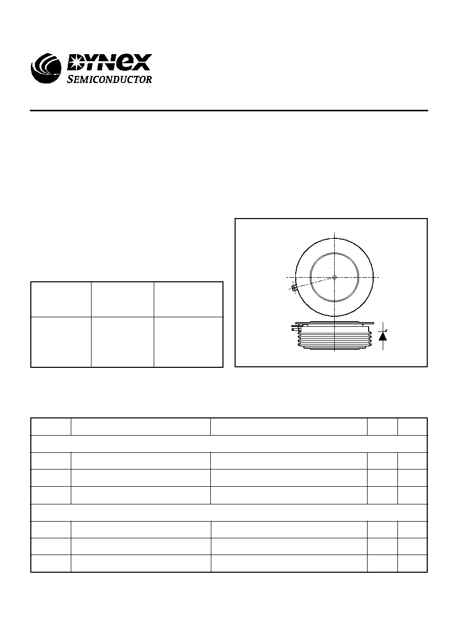
Outline type code: D.
See Package Details for further information.
*Higher dV/dt selections available
DCR1277SD36
DCR1277SD35
DCR1277SD34
DCR1277SD33
DCR1277SD32
Conditions
T
vj
= 0∞ to 125∞C,
I
DRM
= I
RRM
= 150mA,
V
DRM
, V
RRM
t
p
= 10ms,
V
DSM
& V
RSM
=
V
DRM
& V
RRM
+ 100V
respectively
Lower voltage grades available.
Type Number
Repetitive Peak
Voltages
V
DRM
V
RRM
V
CURRENT RATINGS
T
case
= 60∞C unless stated otherwise.
Symbol
Parameter
Conditions
Double Side Cooled
I
T(AV)
Mean on-state current
I
T(RMS)
RMS value
I
T
Continuous (direct) on-state current
Single Side Cooled (Anode side)
I
T(AV)
Mean on-state current
I
T(RMS)
RMS value
I
T
Continuous (direct) on-state current
Units
Max.
Half wave resistive load
1259
A
-
1977
A
-
1832
A
Half wave resistive load
885
A
-
1390
A
-
1209
A
3600
3500
3400
3300
3200
DCR1277SD
Phase Control Thyristor
Replaces March 1998 version, DS4552-3.3
DS4552-4.0 January 2000

DCR1277SD
2/9
SURGE RATINGS
Conditions
10ms half sine; T
case
= 125
o
C
V
R
= 50% V
RRM
- 1/4 sine
10ms half sine; T
case
= 125
o
C
V
R
= 0
Max.
Units
Symbol
Parameter
I
TSM
Surge (non-repetitive) on-state current
I
2
t
I
2
t for fusing
I
TSM
Surge (non-repetitive) on-state current
I
2
t
I
2
t for fusing
2.82 x 10
6
A
2
s
23.75
kA
1.8 x 10
6
A
2
s
19.0
kA
THERMAL AND MECHANICAL DATA
dc
Conditions
Min.
Max.
Units
o
C/W
-
0.036
Anode dc
Clamping force 22.0kN
with mounting compound
Thermal resistance - case to heatsink
R
th(c-h)
0.004
Double side
-
125
o
C
T
vj
Virtual junction temperature
T
stg
Storage temperature range
Reverse (blocking)
Single side
-
Thermal resistance - junction to case
R
th(j-c)
Single side cooled
Symbol
Parameter
Clamping force
20.0
24.0
kN
-55
125
o
C
-
On-state (conducting)
-
135
o
C
-
0.008
o
C/W
o
C/W
Cathode dc
-
0.044
o
C/W
Double side cooled
-
0.020
o
C/W
CURRENT RATINGS
T
case
= 80∞C unless stated otherwise.
Symbol
Parameter
Conditions
Double Side Cooled
I
T(AV)
Mean on-state current
I
T(RMS)
RMS value
I
T
Continuous (direct) on-state current
Single Side Cooled (Anode side)
I
T(AV)
Mean on-state current
I
T(RMS)
RMS value
I
T
Continuous (direct) on-state current
Units
Max.
Half wave resistive load
995
A
-
1565
A
-
1420
A
Half wave resistive load
690
A
-
1085
A
-
920
A

DCR1277SD
3/9
DYNAMIC CHARACTERISTICS
Parameter
Symbol
Conditions
Typ.
Max.
Units
GATE TRIGGER CHARACTERISTICS AND RATINGS
V
DRM
= 5V, T
case
= 25
o
C
Conditions
Parameter
Symbol
V
GT
Gate trigger voltage
V
DRM
= 5V, T
case
= 25
o
C
I
GT
Gate trigger current
V
GD
Gate non-trigger voltage
At V
DRM
T
case
= 125
o
C
4.0
V
400
mA
0.25
V
Max.
Units
I
RRM
/I
DRM
Peak reverse and off-state current
At V
RRM
/V
DRM
, T
case
= 125
o
C
From 67% V
DRM
to 1000A
Gate source 10V, 5
t
r
0.5
µ
s, T
j
= 125
o
C
dV/dt
Maximum linear rate of rise of off-state voltage
To 67% V
DRM
T
j
= 125
o
C.
-
150
mA
-
300
V/
µ
s
Repetitive 50Hz
-
100
A/
µ
s
Non-repetitive
-
150
A/
µ
s
Rate of rise of on-state current
dI/dt
V
T(TO)
Threshold voltage
At T
vj
= 125
o
C
r
T
On-state slope resistance
At T
vj
= 125
o
C
t
gd
Delay time
0.95
-
V
-
0.45
m
-
2.5
µ
s
V
D
= 67% V
DRM
, Gate source 30V, 15
t
r
= 0.5
µ
s, T
j
= 25
o
C
I
T
= 2000A, t
p
= 1ms, T
j
= 125∞C,
V
R
= 50V, dI
RR
/dt = 5A/
µ
s,
V
DR
= 67% V
DRM
, dV
DR
/dt = 20V/
µ
s linear
µ
s
650
500
Turn-off time
t
q
I
L
Latching current
T
j
= 25
o
C, V
D
= 5V
I
H
Holding current
T
j
= 25
o
C, R
g-k
=
700
1000
mA
200
500
mA
V
FGM
Peak forward gate voltage
Anode positive with respect to cathode
V
FGN
Peak forward gate voltage
Anode negative with respect to cathode
V
RGM
Peak reverse gate voltage
I
FGM
Peak forward gate current
Anode positive with respect to cathode
P
GM
Peak gate power
See table, fig.4
P
G(AV)
Mean gate power
30
V
0.25
V
5
V
10
A
150
W
5
W

DCR1277SD
4/9
CURVES
Fig.1 Maximum (limit) on-state characteristics
0.5
1.0
1.5
2.0
Instantaneous on-state voltage V
T
- (V)
0
500
1000
1500
2000
2500
Instantaneous on-state current I
T
- (A)
Measured under pulse conditions
T
j
= 125∞C
3000
2.5

DCR1277SD
5/9
Fig.2 Dissipation curves
0
500
1000
1500
2000
Mean on-state current I
T(AV)
- (A)
0
1000
2000
3000
4000
Mean power dissipation - (W)
d.c.
Half wave
3 phase
6 phase