 | –≠–ª–µ–∫—Ç—Ä–æ–Ω–Ω—ã–π –∫–æ–º–ø–æ–Ω–µ–Ω—Ç: DF65435 | –°–∫–∞—á–∞—Ç—å:  PDF PDF  ZIP ZIP |

DF654
1/7
APPLICATIONS
s
Induction Heating
s
A.C. Motor Drives
s
Inverters And Choppers
s
Welding
s
High Frequency Rectification
s
UPS
FEATURES
s
Double Side Cooling
s
High Surge Capability
s
Low Recovery Charge
VOLTAGE RATINGS
KEY PARAMETERS
V
RRM
3500V
I
F(AV)
675A
I
FSM
6000A
Q
r
900
µ
C
t
rr
6.5
µ
s
CURRENT RATINGS
Symbol
Parameter
Conditions
Double Side Cooled
I
F(AV)
Mean forward current
I
F(RMS)
RMS value
I
F
Continuous (direct) forward current
Single Side Cooled (Anode side)
I
F(AV)
Mean forward current
I
F(RMS)
RMS value
I
F
Continuous (direct) forward current
Units
Max.
Half wave resistive load, T
case
= 65
o
C
675
A
T
case
= 65
o
C
1060
A
T
case
= 65
o
C
960
A
Half wave resistive load, T
case
= 65
o
C
440
A
T
case
= 65
o
C
690
A
T
case
= 65
o
C
600
A
3500
3400
3200
3000
DF654 35
DF654 34
DF654 32
DF654 30
Conditions
V
RSM
= V
RRM
+ 100V
Lower voltage grades available.
Type Number
Repetitive Peak
Reverse Voltage
V
RRM
V
Outline type code: M779b.
See Package Details for further information.
DF654
Fast Recovery Diode
Replaces March 1998 version, DS4214-3.5
DS4214-4.0 January 2000
DF654
2/7
SURGE RATINGS
Conditions
Max.
Units
6.0
kA
180 x 10
3
A
2
s
I
2
t for fusing
I
2
t
Surge (non-repetitive) forward current
I
FSM
Parameter
Symbol
10ms half sine; with 0% V
RRM,
T
j
= 150
o
C
4.8
kA
115 x 10
3
A
2
s
I
2
t for fusing
I
2
t
Surge (non-repetitive) forward current
I
FSM
10ms half sine; with 50% V
RRM,
T
j
= 150
o
C
THERMAL AND MECHANICAL DATA
dc
Conditions
Max.
Units
o
C/W
-
0.086
Anode dc
Clamping force 10kN
with mounting compound
Thermal resistance - case to heatsink
R
th(c-h)
0.01
Double side
-
Single side
Thermal resistance - junction to case
R
th(j-c)
Single side cooled
Symbol
Parameter
-
0.02
o
C/W
o
C/W
Cathode dc
-
0.095
o
C/W
Double side cooled
-
0.045
o
C/W
T
stg
Storage temperature range
-55
150
o
C
kN
11.0
9.0
Clamping force
-
T
vj
Virtual junction temperature
Forward (conducting)
-
150
o
C
Min.
t
rr
60
Symbol
Typ.
Units
Parameter
V
FM
Forward voltage
I
RRM
Peak reverse current
Reverse recovery time
Q
RA1
Recovered charge (50% chord)
I
RM
Reverse recovery current
K
Soft factor
V
TO
Threshold voltage
r
T
Slope resistance
V
FRM
Forward recovery voltage
di/dt = 1000A/
µ
s, T
j
= 125
o
C
-
-
V
At T
vj
= 150
o
C
-
0.9
m
At T
vj
= 150
o
C
-
1.1
V
-
-
-
-
300
A
-
900
µ
C
-
6.5
µ
s
At V
RRM
, T
case
= 150
o
C
-
mA
At 1500A peak, T
case
= 25
o
C
-
2.4
V
Conditions
Max.
I
F
= 1000A, di
RR
/dt = 100A/
µ
s
T
case
= 150
o
C, V
R
= 100V
CHARACTERISTICS

DF654
3/7
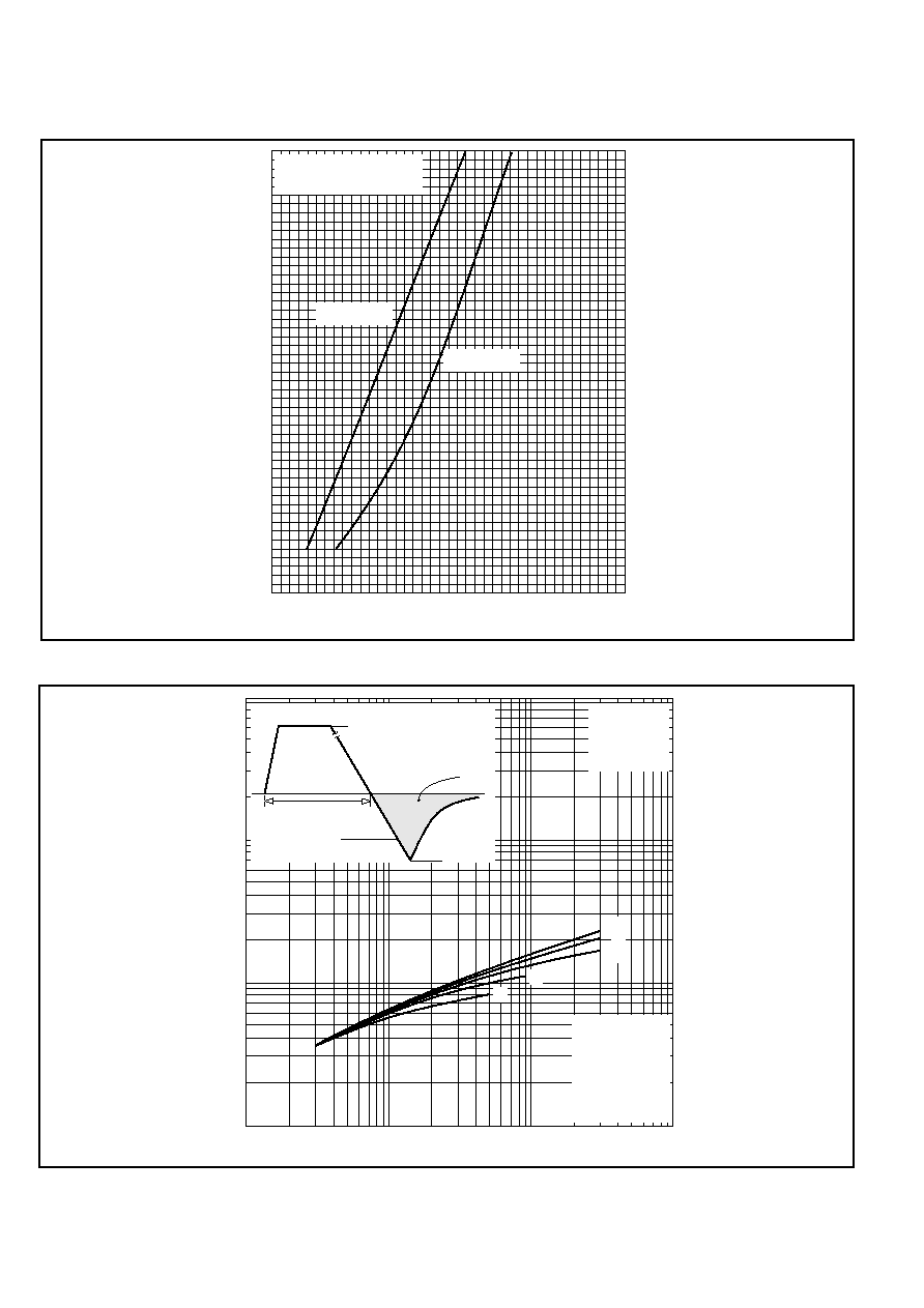
DEFINITION OF K FACTOR AND Q
RA1
0.5x I
RR
I
RR
dI
R
/dt
t
1
t
2
Q
RA1
= 0.5x I
RR
(t
1
+ t
2
)
k = t
1
/t
2
CURVES
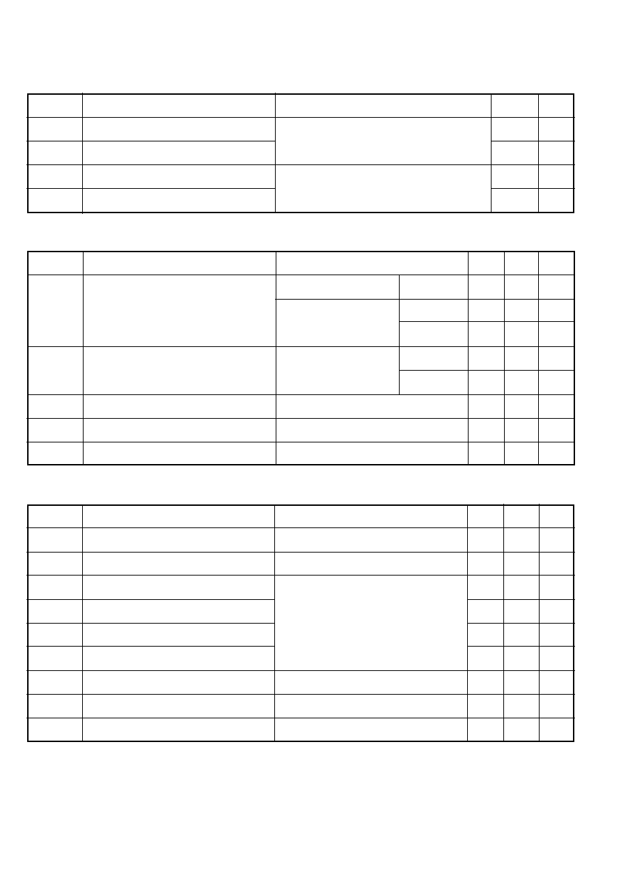
Fig.1 Maximum (limit) forward characteristics
500
1000
1500
2000
2500
3000
Instantaneous forward current I
F
- (A)
1.5
2.0
2.5
3.0
3.5
Instantaneous forward voltage V
F
- (V)
Measured under pulse conditions
T
j
= 150∞C
T
j
= 25∞C
DF654
4/7
Fig.3 Recovered charge
1
10
100
1000
Rate of rise of reverse current dI
R
/dt - (A/
µ
s)
1000
100
10000
100000
Reverse recovered charge Q
S
- (
µ
C)
A: I
F
= 2000A
B: I
F
= 1000A
C: I
F
= 500A
D: I
F
= 200A
E: I
F
= 100A
A
B
C
D
E
I
RR
QS
t
p
= 1ms
I
F
dI
R
/dt
Q
S
=
Conditions:
T
j
= 150 ∞C,
V
R
= 100 V
50
µ
s
0
Fig.2 Maximum (limit) forward characteristics
0
100
200
300
400
500
Instantaneous forward current I
F
- (A)
1.0
1.25
1.5
1.75
2.0
Instantaneous forward voltage V
F
- (V)
Measured under pulse
conditions
T
j
= 150∞C
T
j
= 25∞C
DF654
5/7
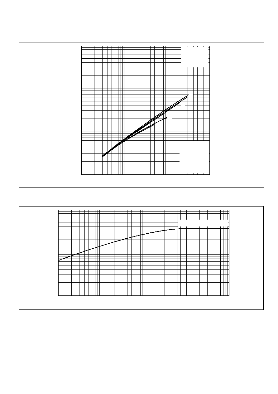
Fig.4 Typical reverse recovery current
1
10
100
1000
Rate of rise of reverse current dI
R
/dt - (A/
µ
s)
100
10
1000
10000
Reverse recovery current I
RR
- (A)
Conditions:
T
j
= 150∞C,
V
R
= 100V
A: I
F
= 2000A
B: I
F
= 1000A
C: I
F
= 500A
D: I
F
= 200A
E: I
F
= 100A
A
B
D
E
C
Fig.5 Maximum (limit) transient thermal impedance - junction to case - (∞C/W)
0.100
0.010
0.001
Thermal impedance - (∞C/W)
0.01
0.1
1
10
100
Time - (s)
d.c. Double side cooled