DF752
1/7
APPLICATIONS
s
Induction Heating
s
A.C. Motor Drives
s
Inverters And Choppers
s
Welding
s
High Frequency Rectification
s
UPS
FEATURES
s
Double Side Cooling
s
High Surge Capability
s
Low Recovery Charge
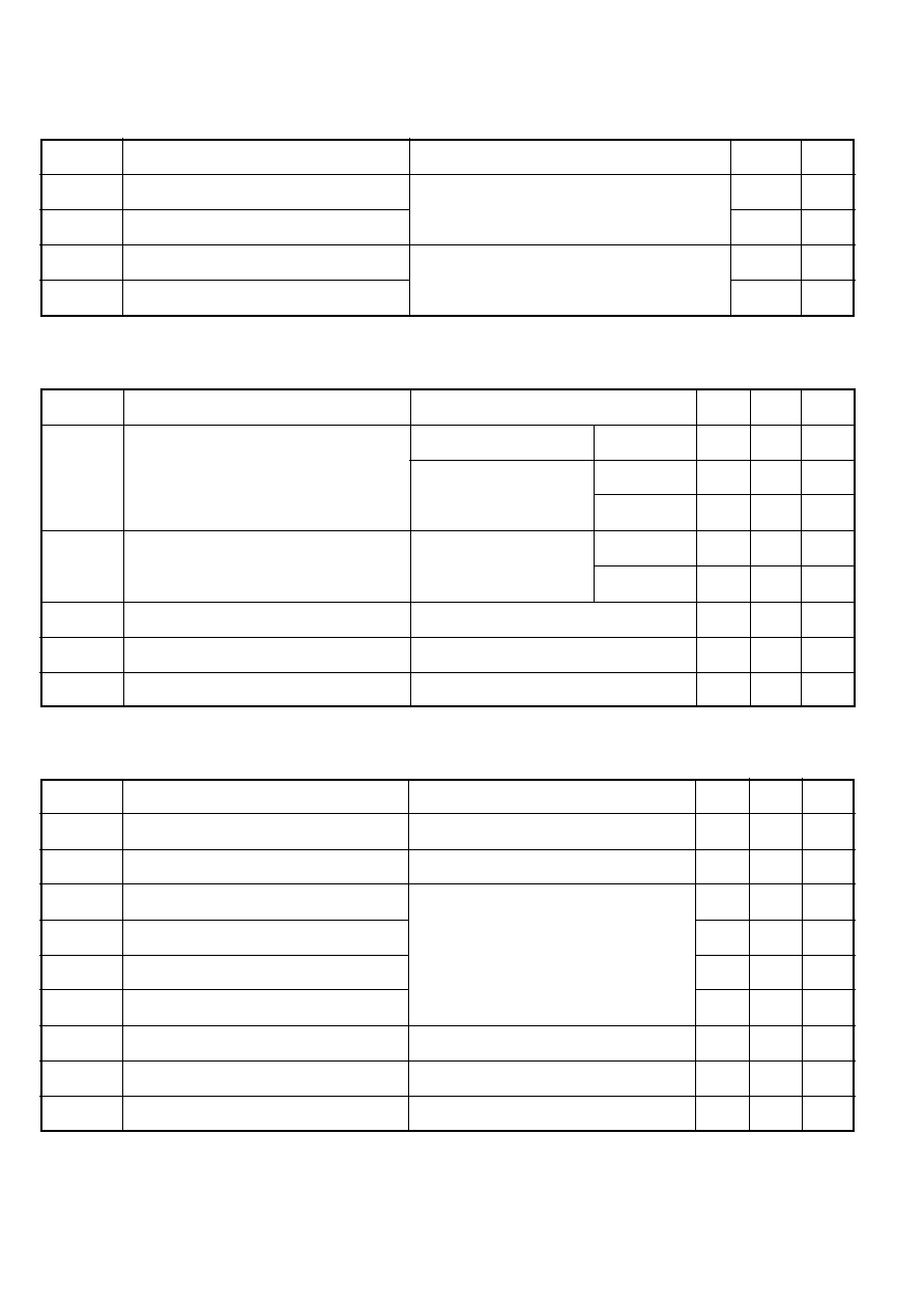
VOLTAGE RATINGS
KEY PARAMETERS
V
RRM
2500V
I
F(AV)
1050A
I
FSM
12000A
Q
r
1000
µ
C
t
rr
6.0
µ
s
CURRENT RATINGS
Symbol
Parameter
Conditions
Double Side Cooled
I
F(AV)
Mean forward current
I
F(RMS)
RMS value
I
F
Continuous (direct) forward current
Single Side Cooled (Anode side)
I
F(AV)
Mean forward current
I
F(RMS)
RMS value
I
F
Continuous (direct) forward current
Units
Max.
Half wave resistive load, T
case
= 65
o
C
1050
A
T
case
= 65
o
C
1660
A
T
case
= 65
o
C
1500
A
Half wave resistive load, T
case
= 65
o
C
686
A
T
case
= 65
o
C
1078
A
T
case
= 65
o
C
933
A
2500
2400
2200
2000
DF752 25
DF752 24
DF752 22
DF752 20
Conditions
V
RSM
= V
RRM
+ 100V
Lower voltage grades available.
Type Number
Repetitive Peak
Reverse Voltage
V
RRM
V
Outline type code: M779b.
See Package Details for further information.
DF752
Fast Recovery Diode
Replaces March 1998 version, DS4212-3.4
DS4548 - 3.2 January 2000
DF752
2/7
SURGE RATINGS
Conditions
Max.
Units
12.0
kA
720 x 10
3
A
2
s
I
2
t for fusing
I
2
t
Surge (non-repetitive) forward current
I
FSM
Parameter
Symbol
10ms half sine; with 0% V
RRM,
T
j
= 150
o
C
9.6
kA
460 x 10
3
A
2
s
I
2
t for fusing
I
2
t
Surge (non-repetitive) forward current
I
FSM
10ms half sine; with 50% V
RRM,
T
j
= 150
o
C
THERMAL AND MECHANICAL DATA
dc
Conditions
Max.
Units
o
C/W
-
0.069
Anode dc
Clamping force 15kN
with mounting compound
Thermal resistance - case to heatsink
R
th(c-h)
0.01
Double side
-
Single side
Thermal resistance - junction to case
R
th(j-c)
Single side cooled
Symbol
Parameter
-
0.02
o
C/W
o
C/W
Cathode dc
-
0.076
o
C/W
Double side cooled
-
0.036
o
C/W
T
stg
Storage temperature range
-55
175
o
C
kN
16.5
13.5
Clamping force
-
T
vj
Virtual junction temperature
On-state (conducting)
-
150
o
C
Min.
t
rr
60
Symbol
Typ.
Units
Parameter
V
FM
Forward voltage
I
RRM
Peak reverse current
Reverse recovery time
Q
RA1
Recovered charge (50% chord)
I
RM
Reverse recovery current
K
Soft factor
V
TO
Threshold voltage
r
T
Slope resistance
V
FRM
Forward recovery voltage
di/dt = 1000A/
µ
s, T
j
= 125
o
C
-
-
V
At T
vj
= 150
o
C
-
0.45
m
At T
vj
= 150
o
C
-
0.9
V
-
-
-
-
330
A
-
1000
µ
C
-
6.0
µ
s
At V
RRM
, T
case
= 150
o
C
-
mA
At 2000A peak, T
case
= 25
o
C
-
1.8
V
Conditions
Max.
I
F
= 1000A, di
RR
/dt = 100A/
µ
s
T
case
= 150
o
C, V
R
= 100V
CHARACTERISTICS

DF752
6/7
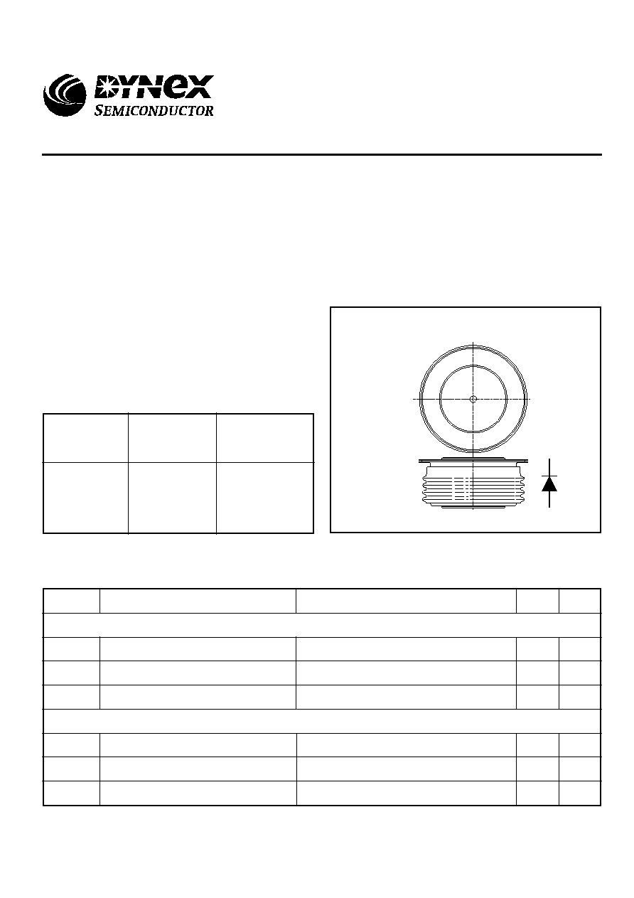
PACKAGE DETAILS
For further package information, please contact your local Customer Service Centre. All dimensions in mm, unless stated otherwise.
DO NOT SCALE.
2 holes ÿ3.6x2.0 deep (in both electrodes)
ÿ34 nom
27.0
25.4
Cathode
Anode
ÿ34 nom
ÿ58.5 max
Nominal weight: 310g
Clamping force: 12kN
±
10%
Package outine type code: M779b
ASSOCIATED PUBLICATIONS
Title
Application Note
Number
Calculating the junction temperature or power semiconductors
AN4506
Recommendations for clamping power semiconductors
AN4839
Thyristor and diode measurement with a multi-meter
AN4853
Use of V
TO
, r
T
on-state characteristic
AN5001

DF752
7/7
POWER ASSEMBLY CAPABILITY
The Power Assembly group was set up to provide a support service for those customers requiring more than the basic semiconduc-
tor, and has developed a flexible range of heatsink / clamping systems in line with advances in device types and the voltage and
current capability of our semiconductors.
We offer an extensive range of air and liquid cooled assemblies covering the full range of circuit designs in general use today. The
Assembly group continues to offer high quality engineering support dedicated to designing new units to satisfy the growing needs of
our customers.
Using the up to date CAD methods our team of design and applications engineers aim to provide the Power Assembly Complete
solution (PACs).
DEVICE CLAMPS
Disc devices require the correct clamping force to ensure their safe operation. The PACs range offers a varied selection of pre-
loaded clamps to suit all of our manufactured devices. This include cube clamps for single side cooling of `T' 22mm
Clamps are available for single or double side cooling, with high insulation versions for high voltage assemblies.
Please refer to our application note on device clamping, AN4839
HEATSINKS
Power Assembly has it's own proprietary range of extruded aluminium heatsinks. They have been designed to optimise the
performance or our semiconductors. Data with respect to air natural, forced air and liquid cooling (with flow rates) is available on
request.
For further information on device clamps, heatsinks and assemblies, please contact your nearest Sales Representative or the
factory.
CUSTOMER SERVICE CENTRES
France, Benelux, Italy and Spain Tel: +33 (0)1 69 18 90 00. Fax: +33 (0)1 64 46 54 50
North America Tel: 011-800-5554-5554. Fax: 011-800-5444-5444
UK, Germany, Scandinavia & Rest Of World Tel: +44 (0)1522 500500. Fax: +44 (0)1522 500020
SALES OFFICES
France, Benelux, Italy and Spain Tel: +33 (0)1 69 18 90 00. Fax: +33 (0)1 64 46 54 50
Germany Tel: 07351 827723
North America Tel: (613) 723-7035. Fax: (613) 723-1518. Toll Free: 1.888.33.DYNEX (39639) /
Tel: (831) 440-1988. Fax: (831) 440-1989 / Tel: (949) 733-3005. Fax: (949) 733-2986.
UK, Germany, Scandinavia & Rest Of World Tel: +44 (0)1522 500500. Fax: +44 (0)1522 500020
These offices are supported by Representatives and Distributors in many countries world-wide.
© Dynex Semiconductor 2000 Publication No. DS4212-4 Issue No. 4.0 January 2000
TECHNICAL DOCUMENTATION ≠ NOT FOR RESALE. PRINTED IN UNITED KINGDOM
HEADQUARTERS OPERATIONS
DYNEX SEMICONDUCTOR LTD
Doddington Road, Lincoln.
Lincolnshire. LN6 3LF. United Kingdom.
Tel: 00-44-(0)1522-500500
Fax: 00-44-(0)1522-500550
DYNEX POWER INC.
Unit 7 - 58 Antares Drive,
Nepean, Ontario, Canada K2E 7W6.
Tel: 613.723.7035
Fax: 613.723.1518
Toll Free: 1.888.33.DYNEX (39639)
This publication is issued to provide information only which (unless agreed by the Company in writing) may not be used, applied or reproduced for any purpose nor form part of any order or contract nor to be regarded as
a representation relating to the products or services concerned. No warranty or guarantee express or implied is made regarding the capability, performance or suitability of any product or service. The Company reserves
the right to alter without prior notice the specification, design or price of any product or service. Information concerning possible methods of use is provided as a guide only and does not constitute any guarantee that such
methods of use will be satisfactory in a specific piece of equipment. It is the user's responsibility to fully determine the performance and suitability of any equipment using such information and to ensure that any publication
or data used is up to date and has not been superseded. These products are not suitable for use in any medical products whose failure to perform may result in significant injury
or death to the user. All products and materials are sold and services provided subject to the Company's conditions of sale, which are available on request.
All brand names and product names used in this publication are trademarks, registered trademarks or trade names of their respective owners.
http://www.dynexsemi.com
e-mail: power_solutions@dynexsemi.com
Datasheet Annotations:
Dynex Semiconductor annotate datasheets in the top right hard corner of the front page, to indicate product status. The annotations are as follows:-
Target Information: This is the most tentative form of information and represents a very preliminary specification. No actual design work on the product has been started.
Preliminary Information: The product is in design and development. The datasheet represents the product as it is understood but details may change.
Advance Information: The product design is complete and final characterisation for volume production is well in hand.
No Annotation: The product parameters are fixed and the product is available to datasheet specification.