 | –≠–ª–µ–∫—Ç—Ä–æ–Ω–Ω—ã–π –∫–æ–º–ø–æ–Ω–µ–Ω—Ç: DNB6311 | –°–∫–∞—á–∞—Ç—å:  PDF PDF  ZIP ZIP |
1/7
www.dynexsemi.com
DNB63
APPLICATIONS
s
Rectification
s
Freewheel Diode
s
DC Motor Control
s
Power Supplies
s
Welding
s
Battery Chargers
FEATURES
s
Double Side Cooling
s
High Surge Capability
VOLTAGE RATINGS
1500
1400
1300
1200
1100
DNB63 15
DNB63 14
DNB63 13
DNB63 12
DNB63 11
Conditions
V
RSM
= V
RRM
+ 100V
Lower voltage grades available.
Type Number
Repetitive Peak
Reverse Voltage
V
RRM
V
DNB63
Rectifier Diode
Replaces January 2000 version, DS4179-5.0
DS4179-6.0 August 2001
KEY PARAMETERS
V
RRM
1500V
I
F(AV)
5794A
I
FSM
57000A
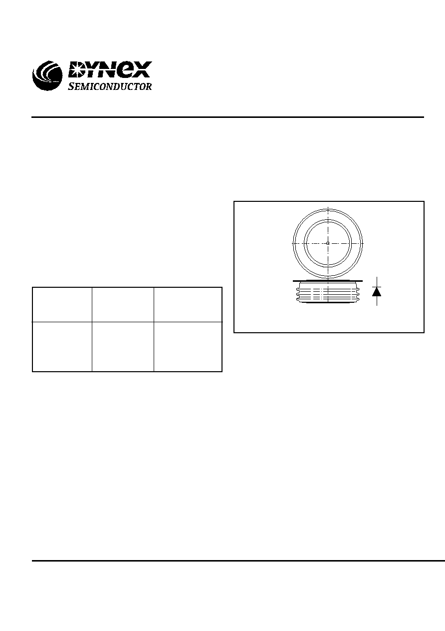
Outline type code: DO200AD
See Package Details for further information.
Fig. 1 Package outline
2/7
www.dynexsemi.com
DNB63
Symbol
Parameter
Conditions
Double Side Cooled
I
F(AV)
Mean forward current
I
F(RMS)
RMS value
I
F
Continuous (direct) forward current
Single Side Cooled (Anode side)
I
F(AV)
Mean forward current
I
F(RMS)
RMS value
I
F
Continuous (direct) forward current
Units
Max.
Half wave resistive load, T
case
= 100
o
C
4850
A
T
case
= 100
o
C
7615
A
T
case
= 100
o
C
6600
A
Half wave resistive load, T
case
= 100
o
C
3540
A
T
case
= 100
o
C
5560
A
T
case
= 100
o
C
4500
A
CURRENT RATINGS
T
case
= 75
o
C unless otherwise stated
Symbol
Parameter
Conditions
Double Side Cooled
I
F(AV)
Mean forward current
I
F(RMS)
RMS value
I
F
Continuous (direct) forward current
Single Side Cooled (Anode side)
I
F(AV)
Mean forward current
I
F(RMS)
RMS value
I
F
Continuous (direct) forward current
Units
Max.
Half wave resistive load
5794
A
-
9101
A
-
7934
A
Half wave resistive load
4230
A
-
6645
A
-
5468
A
T
case
= 100
o
C unless otherwise stated
3/7
www.dynexsemi.com
DNB63
SURGE RATINGS
Conditions
10ms half sine; T
case
= 190
o
C
V
R
= 50% V
RRM
- 1/4 sine
10ms half sine; T
case
= 190
o
C
V
R
= 0
Max.
Units
Symbol
Parameter
I
FSM
Surge (non-repetitive) forward current
I
2
t
I
2
t for fusing
I
FSM
Surge (non-repetitive) forward current
I
2
t
I
2
t for fusing
16.2 x 10
6
A
2
s
57.0
kA
13.5 x 10
6
A
2
s
52.0
kA
THERMAL AND MECHANICAL DATA
dc
Conditions
Min.
Max.
Units
o
C/W
-
0.021
Anode dc
Clamping force 45.0kN
with mounting compound
Thermal resistance - case to heatsink
R
th(c-h)
0.003
Double side
-
T
vj
Virtual junction temperature
T
stg
Storage temperature range
Single side
-
Thermal resistance - junction to case
R
th(j-c)
Single side cooled
Symbol
Parameter
-55
190
o
C
Forward (conducting)
-
o
C
-
0.006
o
C/W
o
C/W
Cathode dc
-
0.034
o
C/W
Double side cooled
-
0.013
o
C/W
Clamping force
40.0
48.0
kN
190
Reverse (blocking)
-
o
C
200
4/7
www.dynexsemi.com
DNB63
CHARACTERISTICS
Forward voltage
Peak reverse current
Parameter
µ
C
4000
Q
S
Total stored charge
Symbol
V
FM
I
RRM
I
RM
Peak recovery current
-
600
A
-
At V
RRM
, T
case
= 190
o
C
-
60
mA
-
1.05
V
At 3000A peak, T
case
= 25
o
C
Conditions
Min.
Max.
Units
At T
vj
= 190∞C
-
V
TO
Threshold voltage
r
T
Slope resistance
0.046
m
At T
vj
= 190∞C
-
0.75
V
t
rr
Reverse recovery time
-
20
µ
s
I
F
= 1000A, dI
RR
/dt = 50A/
µ
s
T
case
= 175∞C, V
R
= 100V
CURVES
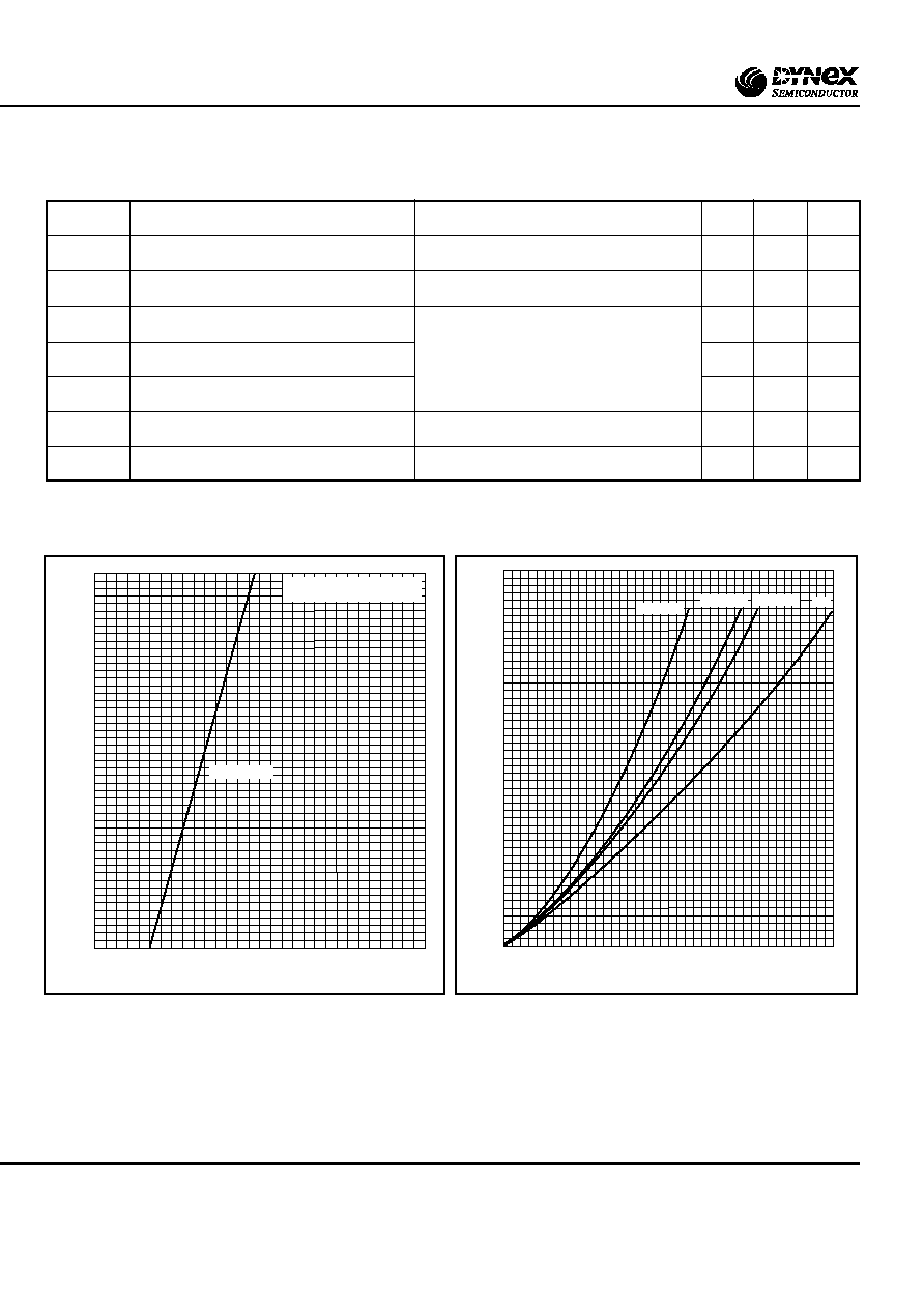
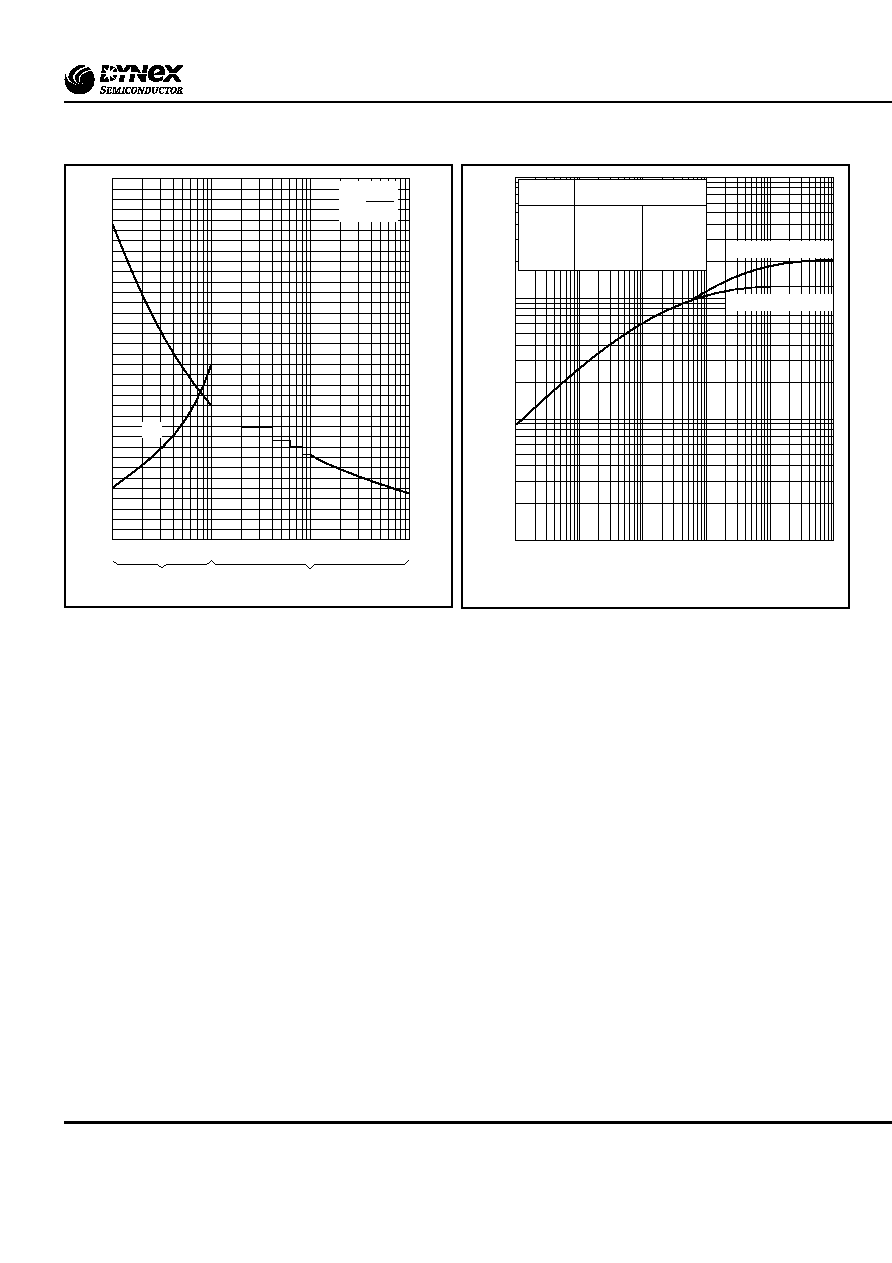
Fig.2 Maximum (limit) forward characteristics
Fig.3 Dissipation curves
V
FM
Equation:-
V
FM
= A + Bln (I
F
) + C.I
F
+D.
I
F
Where
A = 0.517184
B = 0.035583
C = 4.94 x 10
≠5
D = ≠0.0011
these values are valid for T
j
= 125∞C for I
F
500A to 10000A
0.5
1.0
1.5
2.0
Instantaneous forward voltage, V
F
- (V)
0
2000
4000
6000
8000
10000
Instantaneous forward current, I
F
- (A)
Measured under pulse
conditions
T
j
= 190∞C
0
2000
4000
6000
8000
Mean forward current, I
F(AV)
- (A)
0
2000
4000
6000
8000
Mean power dissipation - (W)
dc
Half wave
6 phase
3 phase
10000
5/7
www.dynexsemi.com
DNB63
Fig.5 Maximum (limit) transient thermal impedance -
junction to case
Fig.4 Surge (non-repetitive) forward current vs time (with
50% V
RRM
at T
case
190∞C)
1
10
1
2
3
5
10
20
50
0
20
40
60
80
100
120
10
5
15
I
2
t value - (A
2
s x 10
6
)
ms
Cycles at 50Hz
Duration
Peak half sine forward current - (kA)
I
2
t = Œ
2
x t
2
140
I
2
t
10
1
0.1
0.01
0.001
Time - (s)
0.1
0.01
0.001
0.0001
Thermal impedance - (
∞
C/W)
Double side cooled
Anode side cooled
100
Conduction
d.c.
Halfwave
3 phase 120∞
6 phase 60∞
Effective thermal resistance
Junction to case ∞C/W
Double side
0.0130
0.0141
0.0170
0.0200
Anode side
0.0210
0.0221
0.0250
0.0280