 | –≠–ª–µ–∫—Ç—Ä–æ–Ω–Ω—ã–π –∫–æ–º–ø–æ–Ω–µ–Ω—Ç: MA17502 | –°–∫–∞—á–∞—Ç—å:  PDF PDF  ZIP ZIP |
MA17502
1/30
BLOCK DIAGRAM
The MA17502 Control Unit is a component of the MAS281
chip set. Other chips in the set include the MA17501 Execution
Unit and the MA17503 Interrupt Unit. Also available is the
peripheral MA31751 Memory Management Unit/Block
Protection Unit. In conjunction these chips implement the full
MIL-STD-1750A Instruction Set Architecture.
The MA17502 consisting of a microsequencer, a microcode
storage ROM, and an instruction mapping ROM - controls all
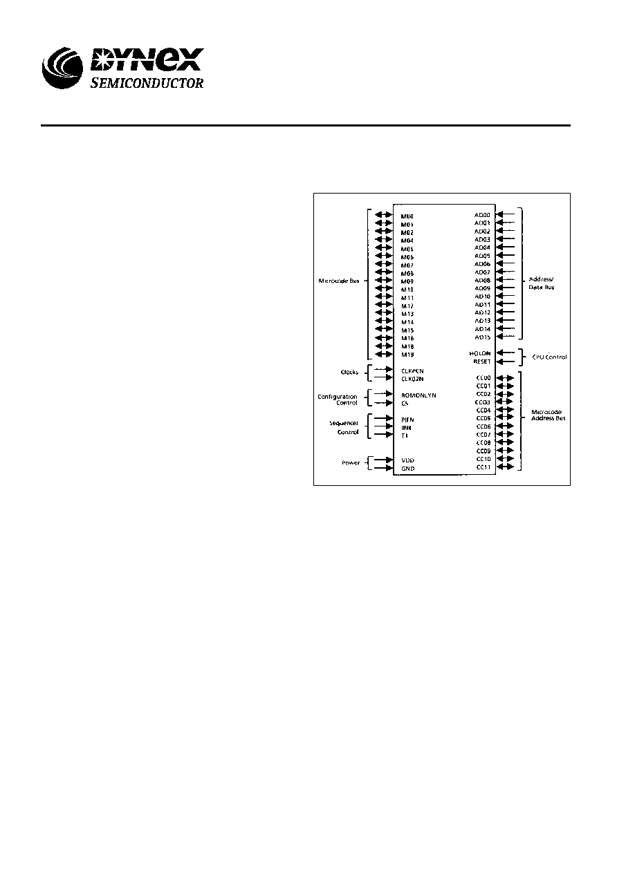
chip set operations. Table 1 provides brief signal definitions.
The MA17502 is offered in several speed and screening
grades, and in dual in-line, flatpack or leadless chip carrier
packaging. Screening options are described in this document.
For availability of speed grades, please contact Dynex
Semiconductor.
FEATURES
s
MIL-STD-1750A Instruction Set Architecture
s
Full Performance Over Military Temperature Range
s
12-Bit Microsequencer
- Instruction Prefetch
- Pipelined Operation
- Subroutine Capability
s
On-Chip ROM
- 2K x 40-Bit Microcode Store
- 512 x 8-Bit Instruction Map
s
MAS281 Integrated Built-In Self Test
s
TTL Compatible System Interface
s
Low Power CMOS/SOS Technology
1.0 SYSTEM CONSIDERATIONS
The MA17502 Control Unit (CU) is a component of the
Dynex Semiconductor MAS281 chip set. The other chips in the
set are the MA17501 Execution Unit (EU) and the MA17503
lnterrupt Unit (lU). Also available is the peripheral MA31751
Memory Management Unit/Block Protection Unit (MMU(BPU)).
The Control Unit, in conjunction with these chips, implements
the full MIL-STD-1750A lnstruction Set Architecture. Figure 1
depicts the relationship between the chip set components.
The CU provides the microprogram storage and
sequencing resources for the chip set. The EU provides the
MAS281's system synchronizing and arithmetic/logic
computational resources. The lU provides interrupt and fault
handling resources, DMA interface control signals, and the
three MIL-STD-1750A timers. The MMU/BPU may be
configured to provide 1M-word memory management (MMU)
and/or 1K-word memory block write protection (BPU) functions.
MA17502
Radiation Hard MIL-STD-1750A Control Unit
Replaces June 1999 version, DS3565-4.0
DS3565-5.0 January 2000
MA17502
2/30
Figure 1: MAS281 Chip Set With Optional MA17504 and Support RAMs
Signature
l/O
Definition
AD00 - AD15
I
External 16-Bit Address/Data Bus
CC00 - CC11
I/O
12-Bit Microcode Address Bus
CLKPC
I
Precharge Clock
CLK02
I
Phase 2 Clock
CS
I
Chip Select
HOLD
I
Hold Request Suspends lnternal Processor Functions
IR
I
Interrupt Request
M00 - M19
I/O/Z
20-Bit Microcode Bus
NC
-
No Connection
PIF
I
Privileged lnstruction Fault
RESET
I
Rest Indicates Device Initialization
ROMONLY
I
Indicates if Control Unit to be Used as ROM Only
T1
I
Branch or Jump Control
VDD
Power (External), 5 Volts
GND
Ground
Table 1: Signal Definitions
MA17501
Execution
Unit
MA17502
Control
Unit
MA17503
Interrupt
Unit
MA31751
Block
Protection
& Memory
Management
Unit
Protection
RAM
128 x 16
Page
RAM
512 x 13
Address
7
Control
1
Data
16
Address
9
Control
1
Data
13
4
3
8
7
16
3
3
20
20
M Bus
16
4
4
7
9
10
1
16
1
16
10
1
8
4
8
Status
Control
Physical Page
Address
Clock
Control
Address/Data
Bus
Control
Control
Faults
Interrupts
Timer
Controls
Power
Reset
MAS281 Chip Set

MA17502
3/30
As shown in Figure 1, the MAS281 is the minimum
processor configuration consisting of an Execution Unit, a
Control Unit, and an Interrupt Unit. This configuration is
capable of accessing a 64K-word address space. Addition of
an MMU configured MA31751 allows access to a 1M-word
address space. This can also be configured as a BPU to
provide hardware support for 1K-word memory block write
protection.
The CU, as with all components of the MAS281 chip set, is
fabricated with CMOS/SOS process technology. Input and
output buffers associated with signals external to the MAS281
are TTL compatible.
Detailed descriptions of the CU's companion chips are
provided in separate data sheets. Additional discussions on
chip set system considerations, interconnection details, and the
Digital Avionics lnstruction Set (DAlS) mix benchmarking
analysis are provided in separate applications notes.
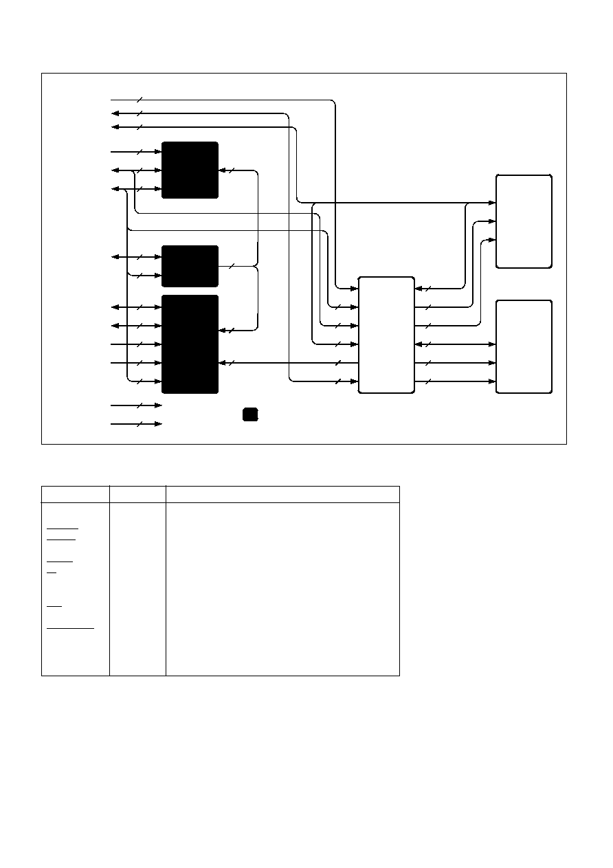
2.0 ARCHITECTURE
The Control Unit consists of a microsequencer, an
instruction mapping ROM, a microcode storage ROM, and
various buses. Details of these components are shown in
Figure 2 and are discussed below:
2.1 MICROSEQUENCER
The CU microsequencer is a 12-bit wide microcode address
generator. Major features of the microsequencer include a
microprogram counter (PC), a microprogram counter save
register (PC Save), microcode address increment logic,
instruction pipeline registers IA and IB, an iteration of loop
counter, a next microcode address source multiplexer, and
various pipelining latches. These features are represented in
Figure 2.
The 12-bit microcode address width allows the
microsequencer to access up to 4096 words of microcode. The
MIL-STD-1750A instructions are implemented as sequences of
microinstructions stored within the lower 2048 locations of this
address space. The address for each microinstruction in a
sequence is provided by the next microcode address source
multiplexer. This multiplexer, under control of the CU control
logic, select from one of six next address sources. Sequential,
direct jump, conditional jump, and subroutine address
generation modes are supported.
Sequential addressing is accomplished by providing a path
from the output of the next microcode address multiplexer to an
incrementer and back to the PC register input. Direct jumps are
supported by routing a portion of the microinstruction to one of
the next microcode address source multiplexer inputs.
Conditional jumps are determined in the ALU of the Execution
Unit which communicates the decision to the CU via the T1
signal. The T1 signal enables a portion of the microcode word
to create the new address. Subroutine jumps are accomplished
by loading the contents of the incremented PC register into the
PC Save register and then performing a direct jump. Upon
completion of the subroutine, the contents of the PC Save
register are used as the next microcode address.
A new microinstruction sequence begins when an opcode
residing in the lA or IB register is selected by the next
microcode address source multiplexer and used as an address
to simultaneously access both the CU's Instruction Mapping
ROM and the Microcode Storage ROM. The instruction
Mapping ROM access provides a pointer which is then used to
update the microprogram counter (PC); the Microcode Storage
ROM access provides the first microinstruction of the
sequence. Remaining microinstructions in a sequence are
accessed through the use of the four address generation
modes discussed above.
Iterative microprogram operations are achieved through the
use of the loop counter. The loop counter may be selectively
loaded from either the AD bus or directly from microcode. This
counter tracks the number of iterations remaining and, when
appropriate, issues a completion signal (CZ). When an iterative
operation is called for, the loop counter is loaded and the CU
control logic repeats a particular microinstruction sequence,
using the four address generation modes discussed above,
until the CZ signal is received.
2.2 INSTRUCTION MAPPING ROM
The CU instruction mapping ROM provides 512 8-bit words
of microcode instruction vector storage. The address space of
this ROM is mapped into a portion of the microcode storage
ROM's address space. Hence, both ROMs are accessed
whenever the microcode address falls within this range. The
eight bits from the instruction mapping ROM serve as-the lower
eight bits of a 12-bit microcode address; the upper four bits are
a hardwired constant. The 12-bit microcode address formed
from the 4-bit constant and the mapping ROM's eight bits are
loaded into the PC register of the microsequencer and serve as
a means to access nonsequential microcode addresses within
the address space allocated to both the instruction mapping
and microcode storage ROMs.
2.3 MICROCODE ROM
The CU microcode ROM provides 2K (2048) 40-bit words of
storage capacity. All of the microcode required to implement
the full MIL-STD-1750A lnstruction Set Architecture (lSA) fits in
one such ROM.
2.4 BUSES
A 16-bit multiplexed Address/Data (AD) bus provides a
communications path between the CU, the other components
of the MAS281 chip set, the MA31751 MMU/BPU, and any
other devices mapped into the chip set's address space. The
CU receives MIL-STD-1750A instructions, accessed from
system memory, over this bus and loads them into its
instruction pipeline registers.
A 20-bit multiplexed Microcode (M) bus provides a pathway
between the CU chip and the microcode decode logic on all
other chips which are under CU microcode control. The 40-bit
wide microinstructions from the CU's microcode ROM are
multiplexed on chip as two 20-bit words and presented on the
interchip M bus during alternate phases of CLK02N. Microcode
bits 39 through 20 are placed on the M bus during the CLK02N
low phase and bits 19 through 0 during the high phase of
CLK02N. The M bus is bidirectional to permit microcode
memory expansion.
A 12-bit microcode address (CC) bus is used to route
microcode addresses from the next microcode address source
multiplexer to the microcode and instruction mapping ROMs as
shown in Figure 2.

MA17502
4/30
3.0 INTERFACE SIGNALS
All signal definitions are shown in Table 1. In addition, each
of these functions is provided with Electrostatic Discharge
(ESD) protection diodes. All unused inputs must be held to their
inactive state via a connection to VDD or GND.
Throughout this data sheet, active low signals are denoted
by either a bar over the signal name or by following the name
with an "N" suffix. e.g. HOLDN. Referenced signals that are not
found on the MA17502 are preceded by the originating chip's
functional acronym in parentheses, e.g. (IU)DMAKN.
A description of each pin function, grouped according to
functional interface, follows. The function acronym is presented
first, followed by its definition, its type, and its detailed
description. Function type is either input, output, high
impedance (Hi-Z), or a combination thereof. Timing
characteristics of each of the functions described are provided
in Section 6.0.
3.1 POWER INTERFACE
The power interface consists of a single 5V VDD connection
and two common GND connections.
3.2 CLOCKS
The clock interface, discussed below, is the means by
which the synchronous, microcoded operation of the MAS281
is driven.
3.2.1 Precharge Clock (CLKPCN)
Input. The MA17501 Execution Unit (EU), generates the
CLKPCN signal for the Control Unit. The Control Unit uses this
signal for most of its internal sequencing. During the low phase
of CLKPCN, the internal M Bus is precharged to the high state
to accelerate its response.
The normal CLKPCN period is defined by five OSC cycles
(two cycles low and three cycles high). When a microcode
branch is indicated by the EU, the low state of CLKPCN is
extended to three OSC cycles. During execution of Interrupt
Unit decoded XlO and microcode commands, the high state of
CLKPCN is extended to four OSC cycles. Also, during external
bus cycles, RDYN may be used to cause the EU to prolong the
high state of CLKPCN to greater than three OSC cycles; this
allows the MAS281 chip set to interface with slower external
memory or input/output devices.
During DMA ((IU)DMAKN is low) or Hold ((EU)HLDAKN is
low), CLKPCN will remain low until the CPU takes control
again.
3.2.2 Phase 2 Clock (CLK02N)
Input. The MA17501 generates the CLK02N signal for the
Control Unit. The CU then uses this signal, in conjunction with
CLKPCN, to control the distribution of microcode on the M Bus.
CLK02N is used to multiplex the 40-bit microcode instruction
into two 20-bit words (
µ
W1 and
µ
W2). The high-to-low edge of
CLK02N switches
µ
W1 (bits 39 through 20) off the M Bus while
switching
µ
W2 (bits 19 through 0) onto the M Bus.
The normal CLK02N period is defined by five OSC cycles
(one cycle low, three cycles high, one cycle low). When a
microcode branch is indicated by the EU, the high state of
CLK02N is extended to four cycles. During execution of
Interrupt Unit decoded XIO and microcode commands, the
trailing low state of CLK02N is extended to two OSC cycles.
Also, during external bus cycles, RDYN may be used to cause
the EU to prolong the CLK02N trailing low state to greater than
one OSC cycle; this allows the MAS281 chip set to interface
with slower external memory or inpuVoutput devices.
During DMA ((IU)DMAKN is low) or Hold ((EU)HLDAKN is
low), CLKPCN will remain low until the CPU takes control
again.
3.3 BUSES
The following is a discussion of the communication buses
connecting the three-chip set. The AD Bus and M Bus are
mainly operand transfer buses, while the CC Bus is strictly for
providing microcode addresses to auxiliary CUs.
3.3.1 Address/Data Bus (AD Bus)
Input. These signals comprise the multiplexed address and
data bus. During external bus operations, the AD bus
accommodates the transfer of instructions, from memory and
l/O ports, to the MA17502. During internal bus operations, the
AD bus provides additional data to the Control Unit from the
Execution Unit. AD00 is the most significant bit position and
AD15 is the least significant bit position of both the 16-bit data
and 16-bit address. A high on this bus corresponds to a logic 1
and a low corresponds to a logic 0. lnformation on the AD Bus is
clocked into the CU by the high-to-low transition of CLKPCN.
3.3.2 Microcode Bus (M Bus)
Input/Output/Hi-z. The M Bus is the 20-bit multiplexed
microcode bus. The 40-bit microcode instruction is multiplexed
onto the M Bus as two 20-bit words (
µ
W1 and
µ
W2). The first
half of the microcode word,
µ
W1 (bits 39 through 20), is
assured valid on the high-to-low transition of CLK02N and
µ
W2
(bits 19 through 0) is assured valid on the high-to-low transition
of CLKPCN. M00 corresponds to microcode bit 0 (
µ
W1) or 20
(
µ
W2) while M19 corresponds to microcode bit 19 (
µ
W1) or 39
(
µ
W2). A high level indicates a logic 1 and a low level indicates
a logic 0. A high level on CS allows the Control Unit to distribute
microcode over this bus, a low level places the bus in the high
impedance state.
During DMA or Hold states, CLKPCN is held low, thus
holding the internal M bus in the precharged state. Precharging
the internal M Bus forces the 20 bits of the external M Bus low.
3.3.3 Microcode Address Bus (CC Bus)
Input/Output/Hi-Z. The CC bus is provided for future
expansion and is left unconnected.
3.4 SEQUENCER CONTROL
The following is a discussion of the microsequencer control
input signals. These signals support chip set functions that
require microcode branching based on the results of operations
performed in the Execution or Interrupt Units.
3.4.1 Interrupt Request (IRN)
Input. A low on this input directs the CU to service pending
interrupt requests latched by the Interrupt Unit (IU). Upon
completion of the currently executing MIL-STD-1750A
instruction, the CU checks the IRN input. If IRN is low, then the
CU sequencer will branch to the microcoded interrupt service
routine; else the next MIL-STD-1750A instruction is mapped to
its microcode routine. The microcoded interrupt service routine

MA17502
5/30
Figure 2: MA17502 Control Unit Architecture