 | –≠–ª–µ–∫—Ç—Ä–æ–Ω–Ω—ã–π –∫–æ–º–ø–æ–Ω–µ–Ω—Ç: MA31751 | –°–∫–∞—á–∞—Ç—å:  PDF PDF  ZIP ZIP |
MA31751
1/17
The MA31751 Memory Management Unit/Block Protect
Unit (MMU/BPU) is an optional chip which may be used to
expand the capabilities of the MA31750.
User configurable, the MA31751 can perform as an MMU,
a BPU or both MMU and BPU, conforming to MIL-STD-1750A
and 1750B. MMU mapping and BPU protection for 1M words
of memory is provided by the internal memory. Up to 16
MA31751 devices can be used to give 16M words of logical
mapped onto 8M words of physical address space with
protection in 1750B mode.
The MA31751 is designed to have a simple interface to
both the CPU and the system bus with the minimal number of
control lines. This reduces board space and simplifies system
design.
The MA31751 traps the MMU and BPU XIO commands to
program and read the logical to physical mapping and memory
access control. This provides simple memory management as
defined by the MIL-STD-1750.
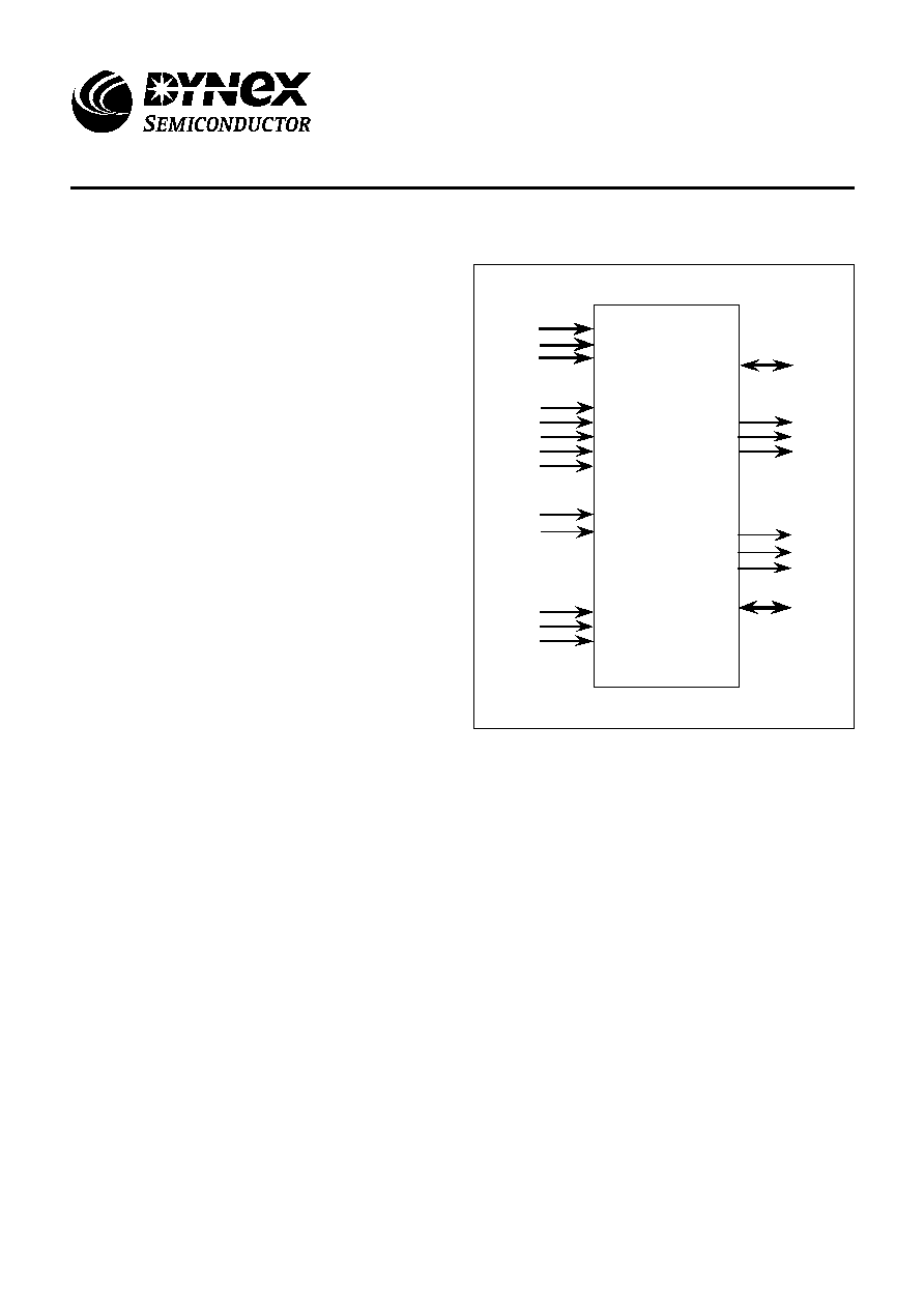
Figure 1: Chip Control Signals
FEATURES
s
MlL-STD-1750A/B Compatible
s
Radiation Hard CMOS/SOS Technology
s
User Configurable as Either a Memory Management Unit
(MMU) or a Block Protect Unit (BPU) or Both
s
Memory Management Unit Configuration
∑ 1 MWord Physical Address Space
∑ Access Lock and Key of 4K-Word Blocks
∑ Write/Execute Protection of 4K-Word Blocks
s
Block Protect Unit Configuration
∑ Protection of 1K-Word Blocks
∑ Global Memory Write Protection During Initialisation
s
Direct Memory Access Support
A[0:15]
AS[0:3]
PS[0:3]
OIN
MION
RDWN
ASIN
DSN
DMAKN
CSN
RESETN
VDD
GND
D[0:16]
PRPEN
MPROEN
GLPE
EA[0:10]
EAS
MA31751
CPU
Busses
Bus
Control
Chip
Control
Signals
System
Signals
System
Faults
BPUVALIDN
HITMISSN
MA31751
Memory Management & Block Protection Unit
Replaces June 1999 version, DS4083-2.0
DS4083-3.0 January 2000
MA31751
2/17
1.0 DEVICE OPERATION
The MA31751 is an interface device designed to increase
the memory addressing capability of the MA31750 CPU. It is
user configurable as an MMU and/or a BPU conforming to the
MIL-STD-1750A and the proposed MIL-STD-1750B. The
MMU provides expanded addressing and full access lock/key
protection in both modes, together with write/execute
protection on 4K pages.
The BPU allows up to 1M words of memory to be protected
in 1K blocks (MlL-STD-1750A). Up to 8M words may be
protected by multiple MMU/BPU units (draft MIL-STD-1750B).
In 1750A mode, one MA31751 unit can act as both MMU
and BPU for the maximum 1M words of address space. In
1750B mode, up to 8 MA31751 units may be used to provide
the maximum BPU functions and up to 16 units for the
maximum MMU functions. For any given physical memory
location the MMU and BPU function may be split across two
MA31751 devices depending on the logical to physical
address mapping.
1.1 INITIALISATION
The MA31751 is initialised by the CPU when a system
reset occurs. Initially all mappings are set one to one to give a
linear 1M word logical to physical mapping. The BPU defaults
to no protection on a reset and requires 256 machine cycles
(AS pulsing) to set the internal BPU memory. The CPU
recognises the presence of the MMU/BPU by the setting of
appropriate bits in the configuration register. When the
configuration register is read, the MA31751 stores MMU, BPU,
parity and 1750 mode information internally. The CPU may
change the mapping and access protection when it is in
privileged instruction mode using XIO commands 4D00 to
52FF as defined in MIL-STD-1750.
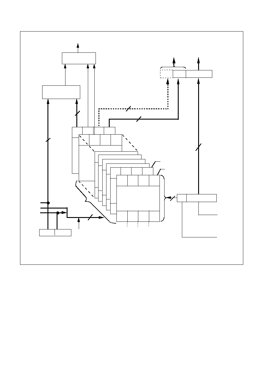
1.2 ADDRESS TRANSLATION AND PROTECTION
The MMU maps system memory into 4K word pages by the
mechanism shown in figure 3. A page is a block of physical
memory which is uniquely specified by the physical page
address, the PPA. A given address within any page is specified
by the least significant 12 bits of the CPU address bus. One
page register has the physical page address and the access
control information relating to one page. There are 512 page
registers, organized into 16 sets. The 16 sets are addressed by
AS[0:3]. Each set has two groups of page registers, one for
operand memory space and one for instruction memory space.
These are addressed by OIN. Each group contains 16 page
registers accommodating a total of 256 registers for each of
operand and instruction memory space.
The MMU also checks for protection violation by
comparing the processor state (PS), read from the CPU status
word, with the access lock (AL) field in the page register. An
additional bit in each page register allows the system to
disable writes to operand pages or reads (execution) of
instruction pages. If any memory violation occurs, the memory
protect output (MPROEN) is asserted low. This typically
causes a bus-fault-timeout on the processor which aborts the
error cycle.
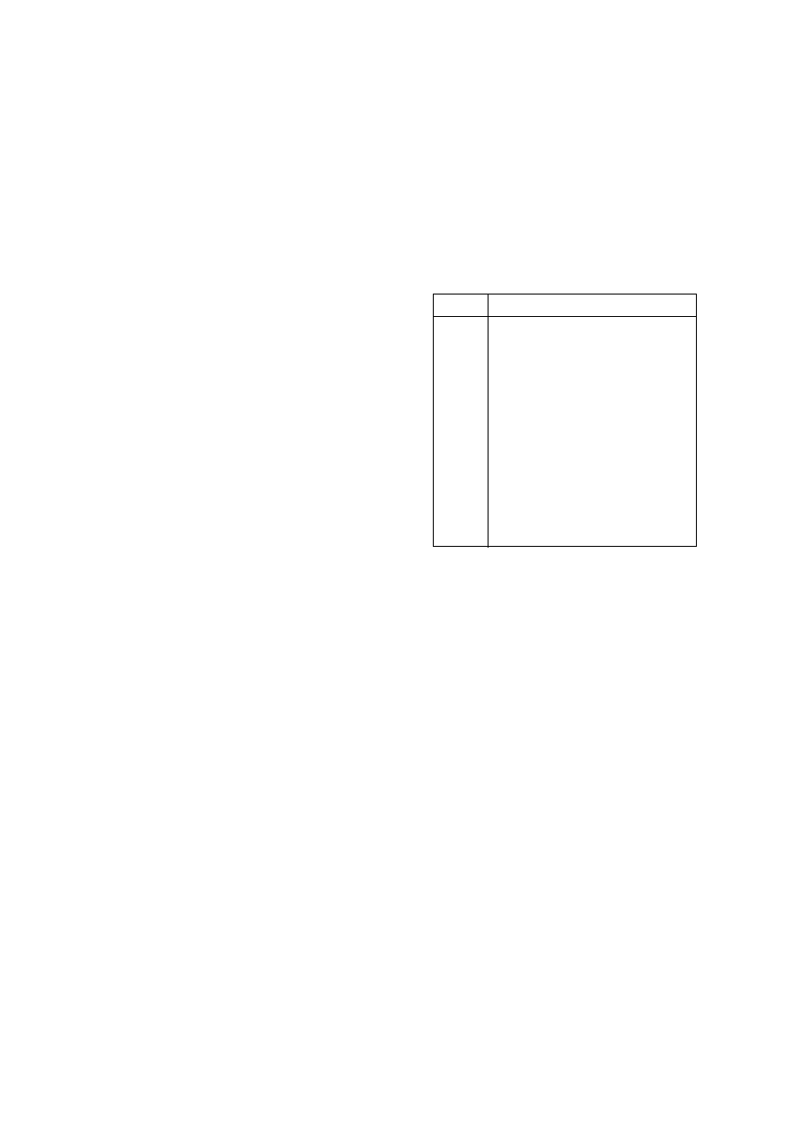
Figure 2 illustrates the Access Key mapping mechanism.
When memory transactions are controlled by the MA31750,
the AS[0:3] and PS[0:3] bits necessary to perform the address
translation and access protection functions respectively, are
obtained from a copy of the processor status word held by the
MMU. Modifications to the CPU status word are reflected in the
MMU copy.
Figure 4 illustrates the standard way to map the logical
CPU addresses, AS[0:3] and PB[0:3] onto the physical
extended address bus for both 1750A (a 20-bit physical
address) and for 1750B (a 23-bit physical address). Figure 5
shows the various selections to achieve the required memory
size and protection.
1.3 BLOCK PROTECTION
The presence of a BPU in the system is determined from
the CPU configuration word. A BPU present in the system
offers protection of the physical memory in 1k blocks. It takes
the physcial address from the EA bus hence the BPU
protection cannot start until the MMU lookup has completed
and EAS rises. If no MMU is present, the physical address is
read from the processor address bus. The address selects the
relevant 16 bit word from the BPU RAM or cache. Each bit in
this word represents the protection on 1k of physical memory.
Any attempt to write a protected block results in an access
violation error from the BPU.
NOTE: MIL-STD-1750 states that the MSB of the Block
Protect Register (BPR) should protect the least significant
address block.
1.4 DIRECT MEMORY ACCESS
The MA31751 supports DMA access within the expanded
memory space, including translation and protection. When a
DMA controller is performing memory transactions, it must
provide the AS[0:3] and PS[0:3] signals to the inputs of the
MMU for address translation and access protection.
AL Code
Acceptable Access Key Codes
0
1
2
3
4
5
6
7
8
9
A
B
C
D
E
F
0
0,1
0,2
0,3
0,4
0,5
0,6
0,7
0,8
0,9
0,A
0,B
0,C
0,D
0,E
0,1,2,3,4,5,6,7,8,9,A,B,C,D,E,F
Figure 2: Access Lock and Key Mapping
MA31751
3/17
AL
E
RES PPA
W
RES
AL
W
RES PPA
PPA
PPA
AL
E
RES PPA
AL
W
RES
PPA
AL
W
RES PPA
AL
W
RES
PPA
0 3 4 5 7 8 15
Instruction
Operand
LPA
4
16-bit logical
address
Address of
word within
4k page
Logical
Address of
4k page
8 bits
12 bits
Extended
Address
Address
8/11-bit address
expansion
12-bit logical
address
8
12
16
words
32
groups
AS
PS
from CPU status word
DMA
AS
PS
DMAKN
5
Group address
OIN
Lock and key
access protection
Protect logic
4
4
Access
violation
*
* These 3 bits are reserved in 1750A. In 1750B they are used as
extra PPA bits to form the MSB's of the extended address bus.
*
*
*
*
MPROEN
Execute
protect
Write
protect
3
3 bits
1750B
12 LSB of Address
Page Register
Page Register
Figure 3: MMU Memory Mapping Mechanism

MA31751
4/17
AS[0:3]
A[0:15]
EA[3:10]
A[4:15]
PB[0:3]
AS[0:3]
A[0:15]
EA[0:10]
A[4:15]
1750A
Addressing
Logical
Physical
1750B
Addressing
Logical*
Physical
1750A Extended Physical Address [0:19]
1750B Extended Physical Address [0:22]
EA3
A4
A15
AS0
AS3 A0
PA0
PA19
EA10
A15
PA0
PA22
A15
A4
EA10
EA0
PB0
PB3
AS3
AS0
A15
A0
* There are 16M words of logical address in 1750B. The 16MWord
logical to 8MWord physical mapping is user defined.
Figure 4: Extended Address Mapping in 1750A/B Mode
Figure 5: MA31751 Selection Chart for Varying Memory Requirements
Addressable
Physical
Memory
Addressable
Logical
Memory
Is BPU
Protection
Required?
Mode
Number of
MMUs
Number of
BPUs
Number of
MA31751s
Required
64KW
64KW
NO
A
0
0
0
1MW
1MW
NO
A
1
0
1
64KW
64KW
YES
A
0
1
1
1MW
1MW
YES
A
1
1
1
64KW
64KW
NO
B
0
0
0
8MW
1MW
NO
B
1
0
1
8MW
2MW
NO
B
2
0
2
8MW
4MW
NO
B
4
0
4
8MW
8MW
NO
B
8
0
8
8MW
16MW
NO
B
16
0
16
64KW
64KW
YES
B
0
1
1
8MW
1MW
YES
B
1
8
8
8MW
2MW
YES
B
2
8
8
8MW
4MW
YES
B
4
8
8
8MW
8MW
YES
B
8
8
8
8MW
16MW
YES
B
16
8
16
Notes: 1. Memory is specified in terms of addressable instruction space.
2. It is assumed that the whole of the physical address space is used in 1750B - if this is not the
case the number of MA31751 chips may be reduced.

MA31751
5/17
2.0 TIMING CONSIDERATIONS
2.1 MMU TIMINGS
To enable a fast page register look-up time, the MMU has
two fast translation cache registers. These hold the address
translation information on the 4K memory page which is
currently being accessed. When the CPU has control of the
system, one cache register is for operand transfers and one for
instruction transfers, as these often occur in different pages.
The appropriate translation cache register is chosen by the
operand/instruction (OIN) signal from the CPU. When a DMA
has system control, the caches operate as Read/Write caches,
the appropriate cache being selected by the RDWN signal.
When either an instruction/read or an operand/write crosses a
page boundary, one wait state may be added whilst the
translation cache register is updated from internal memory.
This system minimises the MMU overhead.
2.2 BPU TIMINGS
A similar caching system is employed in the BPU section
of the MA31751 to allow more rapid detection of access
violations. If the physical address crosses a 16K block
boundary, then one wait state may be added.
Different combinations of cache hits and misses give
different access times if the MA31751 is acting as both an
MMU and a BPU. If the logical address (from the CPU) gives
an MMU cache hit, the physical address is looked-up from the
translation cache register (operand or instruction, depending
on OIN). If the physical address gives a cache hit, the
protection for the block is looked-up in the BPU cache register.
This situation (both hits) gives the fastest access time. The
access time is a maximum if both logical and physical
addresses give cache misses.
3.0 OUTPUTS FROM THE MA31751
3.1 PRPEN
This signal goes active low if a parity error occurs on a
memory access, ie. there is a parity error in the MMU page
register. There is no parity checking on XIO cycles, (this
should be covered by the processor).
3.2 MPROEN
This signal is always low when ASIN is low. On a memory
access, with an MMU only present it stays low until the
address translation is validated. If the translation is erroneous,
it stays low, causing a machine cycle time-out. If a BPU is
present with the MMU, an erroneous translation causes the
output to stay low. If the translation is correct, MPROEN will
still stay low until the BPU check has completed. If there is no
block protection set, MPROEN goes high, allowing the cycle to
proceed. If the block protection is set, MPROEN stays low and
the cycle times out. In a BPU only system, MPROEN indicates
whether or not the protection bit is set for the address being
accessed.
In a 1750B system with both an MMU and BPU present,
MPROEN may glitch between the translation validation and
the protection check (as the MMU and BPU functions may be
on different devices). In this case, MPROEN should be gated
with BPUVALIDN being low before being input to the CPU.
3.3 BPUVALIDN
BPUVALIDN falls to indicate that the output from the BPU
is valid. If no BPU is present, BPUVALIDN remains high.
4.0 PIN DESCRIPTIONS
A description of each pin function appears in Figure 6. The
acronym is presented first, followed by its function and
description. Timing characteristics of each of the functions are
shown in section 6.
All CMOS compatible signals are protected by an
Electrostatic Discharge (ESD) protection circuit. Throughout
this data sheet, active low signals are denoted either by
placing a bar over the signal name,or by following the signal
name with an "N" suffix, e.g.,DSN.
All unused inputs should be connected to their inactive
state and should not be allowed to float.