 | –≠–ª–µ–∫—Ç—Ä–æ–Ω–Ω—ã–π –∫–æ–º–ø–æ–Ω–µ–Ω—Ç: MA5114 | –°–∫–∞—á–∞—Ç—å:  PDF PDF  ZIP ZIP |
MA5114
1/12
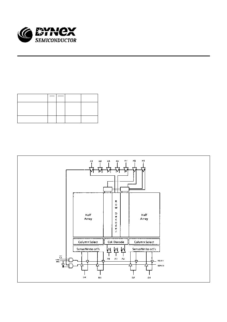
The MA5114 4k Static RAM is configured as 1024 x 4 bits and
manufactured using CMOS-SOS high performance, radiation hard,
3
µ
m technology.
The design uses a 6 transistor cell and has full static operation with
no clock or timing strobe required. Address input buffers are deselected
when Chip Select is in the HIGH state.
FEATURES
s
3
µ
m CMOS-SOS Technology
s
Latch-up Free
s
Fast Access Time 90ns Typical
s
Total Dose 10
6
Rad(Si)
s
Transient Upset >10
10
Rad(Si)/sec
s
SEU <10
-10
Errors/bitday
s
Single 5V Supply
s
Three State Output
s
Low Standby Current 50
µ
A Typical
s
-55
∞
C to +125
∞
C Operation
s
All Inputs and Outputs Fully TTL or CMOS
Compatible
s
Fully Static Operation
s
Data Retention at 2V Supply
Figure 2: Block Diagram
Operation Mode
CS
WE
I/O
Power
Read
L
H
D OUT
ISB1
Write
L
L
D IN
Standby
H
X
High Z
ISB2
Figure 1: Truth Table
MA5114
Radiation hard 1024x4 Bit Static RAM
Replaces June 1999 version, DS3591-4.0
DS3591-5.0 January 2000
MA5114
2/12
Symbol
Parameter
Min.
Max.
Units
V
CC
Supply Voltage
-0.5
7
V
V
I
Input Voltage
-0.3
V
DD
+0.3
V
T
A
Operating Temperature
-55
125
∞
C
T
S
Storage Temperature
-65
150
∞
C
Figure 3: Absolute Maximum Ratings
Stresses above those listed may cause permanent
damage to the device. This is a stress rating only and
functlonal operation of the device at these condltions,
or at any other condition above those indicated in the
operations section of this specification, is not Implied
Exposure to absolute maxlmum rating conditions for
extended perlods may affect device reliability.
Notes for Tables 4 and 5:
1. Characteristics apply to pre radiation at T
A
= -55
∞
C to +125
∞
C with V
DD
= 5V
±
10% and to post 100k Rad(Si) total dose
radiation at T
A
= 25
∞
C with V
DD
= 5V
±
10% (characteristics at higher radiation levels available on request).
2. Worst case at T
A
= +125
∞
C, guaranteed but not tested at T
A
= -55
∞
C.
GROUP A SUBGROUPS 1, 2, 3.
Symbol
Parameter
Conditions
Min.
Typ.
Max.
Units
V
DD
Supply voltage
-
4.5
5.0
5.5
V
V
lH
Input High Voltage
-
V
DD
/2
-
V
DD
V
V
lL
Input Low Voltage
-
V
SS
-
0.8
V
V
OH
Output High Voltage
I
OH1
= -1mA
2.4
-
-
V
V
OL
Output Low Voltage
I
OL
= 2mA
-
-
0.4
V
I
LI
Input Leakage Current (note 2)
All inputs except
CS
-
-
±
10
µ
A
I
LO
Output Leakage Current (note 2)
Output disabled, V
OUT
= V
SS
or V
DD
-
-
±
20
µ
A
I
PUI
Input Pull-Up Current
V
IN
= V
SS
on
CS
input only
-
-
-100
µ
A
I
PDI
Input Leakage Current
V
IN
= V
SS
on
CS
input only
-
-
5
µ
A
I
DD
Power Supply Current
f
RC
= 1MHz,
CS
= 50% mark:space-
12
16
mA
I
SB1
Selected Supply Current
CS
= V
SS
-
25
35
mA
I
SB2
Standby Supply Current
Chip disabled
-
50
3000
µ
A
Figure 4: Electrical Characteristics
Symbol
Parameter
Conditions
Min.
Typ.
Max.
Units
V
DR
V
CC
for Data Retention
CS
= V
DR
2.0
-
-
V
I
DDR
Data Retention Current
CS
= V
DR
, V
DR
= 2.0V
-
30
2000
µ
A
Figure 5: Data Retention Characteristics
CHARACTERISTICS AND RATINGS
MA5114
3/12
AC CHARACTERISTICS
Conditions of Test for Tables 5 and 6:
1. Input pulse = V
SS
to 3.0V.
2. Times measurement reference level = 1.5V.
3. Transition is measured at
±
500mV from steady state.
4. This parameter is sampled and not 100% tested.
Notes for Tables 6 and 7:
Characteristics apply to pre-radiation at T
A
= -55
∞
C to +125
∞
C with V
DD
= 5V
±
10% and to post 100k Rad(Si) total dose radiation
at T
A
= 25
∞
C with V
DD
= 5V
±
10%. GROUP A SUBGROUPS 9, 10, 11.
Symbol
Parameter
Min
Max
Units
T
AVAVR
Read Cycle Time
135
-
ns
T
AVQV
Address Access Time
-
135
ns
T
ELQV
Chip Select to Output Valid
-
135
ns
T
ELQX
(3,4)
Chip Select to Output Active
10
-
ns
T
ELQZ
(3,4)
Chip Select to Output Tri State
10
50
ns
T
AXQX
Output Hold from Address Change
10
-
ns
Figure 6: Read Cycle AC Electrical Characteristics
Symbol
Parameter
Min
Max
Units
T
AVAVW
Write Cycle Tlme
135
-
ns
T
AVWL
Address Set Up Time
10
-
ns
T
WLWH
Write Pulse Width
50
-
ns
T
WHAV
Write Recovery Time
5
-
ns
T
DVWH
Data Set Up Time
35
-
ns
T
NHDX
Data Hold Time
5
-
ns
T
WLQZ
(3,4)
Write Enable to Output Tri State
10
50
ns
T
ELWL
Chip Selection to Write Low
25
-
ns
T
ELWH
Chip Selection to End of Write
85
-
ns
T
AVWH
Address Valid to End of Write
80
-
ns
T
WHQX
(3,4)
Output Active from End to Write
5
-
ns
Figure 7: Write Cycle AC Electrical Characteristics
Symbol
Parameter
Conditions
Min.
Typ.
Max.
Units
C
IN
Input Capacitance
V
l
= 0V
-
6
10
pF
C
OUT
Output Capacitance
V
O
= 0V
-
8
12
pF
Note: T
A
= 25
∞
C and f = 1MHz. Data obtained by characterisation or analysis; not routinely measured.
Figure 8: Capacitance

MA5114
4/12
Symbol
Parameter
Conditions
F
T
Basic Functionality
V
DD
= 4.5V - 5.5V, FREQ = 1MHz
V
IL
= V
SS
, V
IH
= V
DD
, V
OL
1.5V, V
OH
1.5V
TEMP = -55
∞
C to +125
∞
C, GPS PATTERN SET
GROUP A SUBGROUPS 7, 8A, 8B
Figure 9: Functionality
Subgroup
Definition
1
Static characteristics specified in Tables 4 and 5 at +25
∞
C
2
Static characteristics specified in Tables 4 and 5 at +125
∞
C
3
Static characteristics specified in Tables 4 and 5 at -55
∞
C
7
Functional characteristics specified in Table 9 at +25
∞
C
8A
Functional characteristics specified in Table 9 at +125
∞
C
8B
Functional characteristics specified in Table 9 at -55
∞
C
9
Switching characteristics specified in Tables 6 and 7 at +25
∞
C
10
Switching characteristics specified in Tables 6 and 7 at +125
∞
C
11
Switching characteristics specified in Tables 6 and 7 at -55
∞
C
Figure 10: Definition of Subgroups
MA5114
5/12
TIMING DIAGRAMS
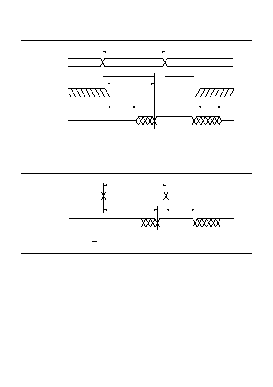
Figure 11a: Read Cycle 1
1.
WE
is high for Read Cycle.
2. Address Vaild prior to or coincident with
CS
transition low.
T
AVAVR
T
AVQV
T
AXQX
T
ELQV
T
ELQX
T
EHQZ
ADDRESS
CS
DATA OUT
HIGH
IMPEDANCE
DATA VALID
Figure 11b: Read Cycle 2
1.
WE
is high for Read Cycle.
2. Device is continually selected.
CS
low.
T
AVAVR
T
AVQV
T
AXQX
ADDRESS
DATA OUT
DATA VALID