 | –≠–ª–µ–∫—Ç—Ä–æ–Ω–Ω—ã–π –∫–æ–º–ø–æ–Ω–µ–Ω—Ç: MAS110S | –°–∫–∞—á–∞—Ç—å:  PDF PDF  ZIP ZIP |
MAS110S
1/9
APPLICATIONS
q
High Frequency High Power Choppers And Inverters.
q
Ultrasonic Generators.
q
Welding.
q
PWM Inverters.
DESCRIPTION
The MAS 110S is a fast thyristor/diode module in an
electrically isolated package. The semiconductors are are
pressure contact mounted giving high resistance to
thermal fatigue, and having excellent heat dissipation
qualities.
Isolation medium is non-toxic alumina.
The MAS110S is recognised under the 'Recognised
Component Program of Underwriters Laboratories Inc.
USA. File number E151069.
VOLTAGE RATINGS
KEY PARAMETERS
V
DRM
1400V
I
TSM
2000A
I
T(AV)
per arm
110A
V
isol
2500V
t
q
10/12/15
µ
s
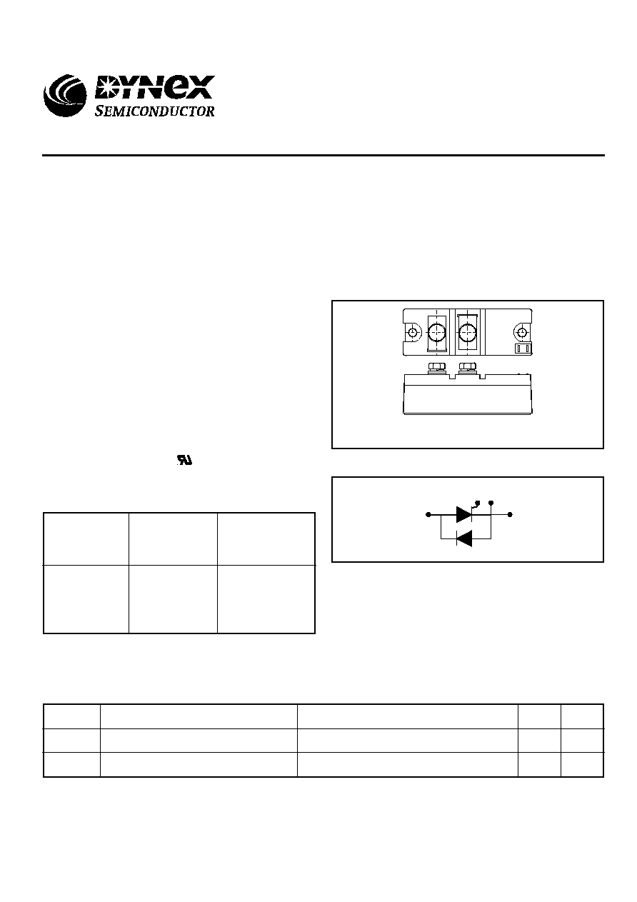
Fig.2 Single circuit
Conditions
T
vj
= 125∞C,
I
DRM
= 50mA,
V
DSM
= V
DRM
+ 100V
For full description of part number see 'Ordering Information'.
Type Number
MAS110S 14
MAS110S 12
MAS110S 10
MAS110S 08
MAS110S 06
Repetitive Peak
Off-state Voltage
V
DRM
V
1400
1200
1000
800
600
Outline type code: MAS110S
See Package Details for further information.
THYRISTOR CURRENT RATINGS
Symbol
Parameter
Conditions
Units
Max.
I
T(AV)
Mean forward current
I
T(RMS)
RMS value
Half wave resistive load, T
case
= 75
o
C
110
A
T
case
= 75
o
C
175
A
G
1
K
1
1
2
Fig.1 Package outline (not to scale)
MAS110S
Fast Turn-off Asymmetric Thyristor/Diode Module
Replaces April 1999 version, DS4200-4.0
DS4200-5.0 January 2000

MAS110S
2/9
THYRISTOR SURGE RATINGS
Conditions
10ms half sine; T
case
= 125
o
C
V
R
= 0% V
DRM
Max.
Units
Symbol
Parameter
I
TSM
Surge (non-repetitive) on-state current
I
2
t
I
2
t for fusing
20.0 x 10
3
A
2
s
2.0
kA
THYRISTOR DYNAMIC CHARACTERISTICS
V
TM
Parameter
Symbol
Conditions
Maximum on-state voltage
At 600A peak, T
case
= 25
o
C
I
DRM
Peak off-state current
At V
DRM
, T
case
= 125
o
C
dV/dt
Maximum linear rate of rise of off-state voltage
To 60% V
DRM
T
j
= 125
o
C, Gate open circuit
Min.
Max.
Units
-
2.9
V
-
70
mA
-
1000
V/
µ
s
Repetitive 50Hz
-
500
A/
µ
s
Rate of rise of on-state current
dI/dt
From 67% V
DRM
to 600A,
Gate source 20V, 20
t
r
= < 0.5
µ
s, T
j
= 125∞C
V
T(TO)
Threshold voltage
At T
vj
= 125
o
C
r
T
On-state slope resistance
At T
vj
= 125
o
C
1.6
-
V
-
1.4
m
Turn-off time
t
q
µ
s
10
-
µ
s
12
-
µ
s
15
-
I
T
= 100A, T
j
= 125∞C,
dI
R
/dt = 30A/
µ
s, V
GK
= 0V
dV/dt = 20V/
µ
s to 60%
V
DRM
, V
R
= 1V.
t
q
code: W
t
q
code: S
t
q
code: X

MAS110S
3/9
DIODE CURRENT RATINGS
Symbol
Parameter
Conditions
Units
Max.
I
T(AV)
Mean forward current
I
T(RMS)
RMS value
Half wave resistive load, T
case
= 75
o
C
112
A
T
case
= 75
o
C
175
A
DIODE SURGE RATINGS - PER ARM
Conditions
10ms half sine; T
case
= 130
o
C
V
R
= 0% V
RRM
Max.
Units
Symbol
Parameter
I
FSM
Surge (non-repetitive) forward current
I
2
t
I
2
t for fusing
61.25 x 10
3
A
2
s
3.5
kA
Conditions
At 600A, T
case
= 25∞C.
Max.
Units
Symbol
Parameter
V
FM
Forward voltage
I
RRM
Peak reverse current
70
mA
2.65
V
At V
RRM
, T
case
= 125∞C.
t
rr
Reverse recovery time
1.3
µ
s
T
case
= 125∞C, dI
R
/dt = -50V/
µ
s, I
FM
= 200A
V
TO
Threshold voltage
1.6
V
At T
vj
= 125∞C.
Forward slope resistance
1.5
m
At T
vj
= 125∞C.
r
T
DIODE DYNAMIC CHARACTERISTICS
THYRISTOR GATE TRIGGER CHARACTERISTICS AND RATINGS
V
DRM
= 12V, T
case
= 25
o
C
Conditions
Parameter
Symbol
V
GT
Gate trigger voltage
V
DRM
= 12V, T
case
= 25
o
C, R
L
= 30
I
GT
Gate trigger current
V
RGM
Peak reverse gate voltage
I
FGM
Peak forward gate current
Anode positive with respect to cathode
P
GM
Peak gate power
-
P
G(AV)
Mean gate power
-
4.0
V
-
250
mA
-
7.0
V
-
10
A
-
50
W
-
15
W
Typ.
Max.
Units
Average timing = 10ms

MAS110S
4/9
THERMAL AND MECHANICAL DATA
Conditions
Min.
Max.
Units
Thermal resistance - junction to case
(Thyristor or diode)
R
th(j-c)
Symbol
Parameter
dc
o
C/W
0.21
-
Mounting force 6Nm
with mounting compound.
Thermal resistance - case to heatsink
(Thyristor or diode)
0.07
-
o
C/W
R
th(c-h)
125
o
C
T
vj
Virtual junction temperature
T
stg
Storage temperature range
V
isol
Isolation voltage
-
2.5
kV
-40
125
o
C
-40
-
-
125
o
C
-
T
op
Operating temperature range
Commoned terminals to base plate.
AC RMS, 1 min, 50Hz.
-
Mounting torque
-
6.0
Nm
ORDERING INFORMATION
The module type number is made up as follows:
MAS XXX S XX W
Nominal I
F(AV)
at T
case
= 75∞C
Single thyristor/diode configuration
Voltage grade. V
DRM
/100
Turn-off time code
Examples:
MAS 110 S 12 W
MAS 110 S 08 X
MODULE MOUNTING RECOMMENDATIONS
s
Adequate heatsinking is required to maintain the base
temperature at 75
o
C if full rated current is to be achieved. Power
dissipation may be calculated by use of V
T(TO)
and r
T
information
and loss curves in accordance with standard formulae. We can
provide assistance with calculations or choice of heatsink if required.
s
The heatsink surface must be smooth and flat; a surface finish
of N6 (32
µ
in) and a flatness within 0.05mm (0.002") are
recommended.
s
Immediately prior to mounting, the heatsink surface should be
lightly scrubbed with fine emery, Scotch BriteTM or a mild chemical
etchant and then cleaned with a solvent to remove oxide build up
and foreign material. Care should be taken to ensure no foreign
particles remain.
s
An even coating of thermal compound (eg. Unial) should be
applied to both the heatsink and module mounting surfaces. This
should ideally be 0.05mm (0.002") per surface to ensure optimum
thermal performance.
s
After application of thermal compound, place the module squarely
over the mounting holes, (or 'T' slots) in the heatsink. Using a
torque wrench, slowly tighten the recommended fixing bolts at
each end, rotating each in turn no more than 1/4 of a revolution at
a time. Continue until the required torque of 6Nm (55lb.ins) is
reached at both ends.
s
It is not acceptable to fully tighten one fixing bolt before starting
to tighten the others. Such action may DAMAGE the module.
Pressure contact asymmetric thyristor/diode module
MAS110S
5/9
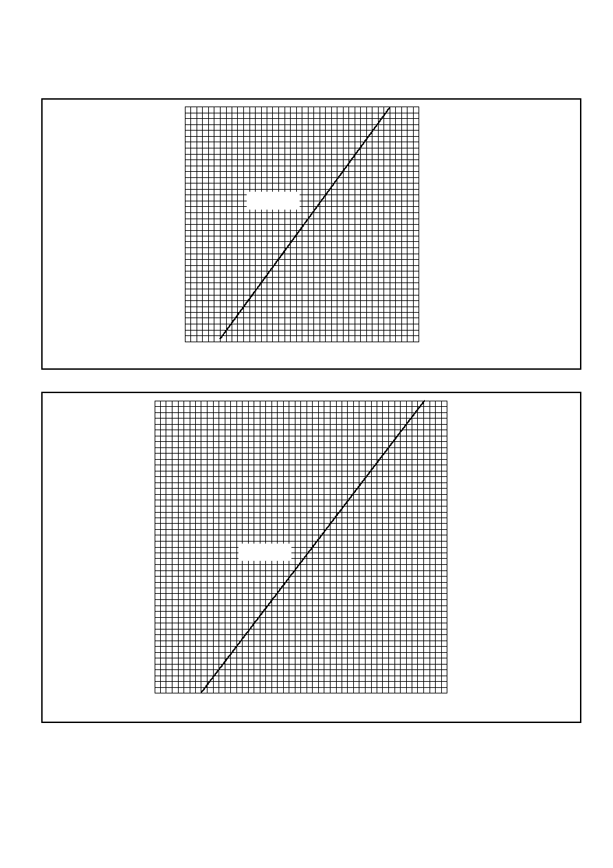
Curves
0
2.0
4.0
6.0
8.0
Instantaneous forward voltage V
F
- (V)
0
1000
2000
3000
4000
5000
Instantaneous forward current I
F
- (A)
Tj = 125∞C
10.0
1.0
2.0
3.0
4.0
5.0
Instantaneous on-state voltage V
T
- (V)
0
500
1000
1500
2000
Instantaneous on-state current I
T
- (A)
T
j
= 125∞C
Fig.3 Maximum (limit) on-state characteristics (thyristor only)
Fig.4 Maximum (limit) forward characteristics (diode only)
MAS110S
6/9
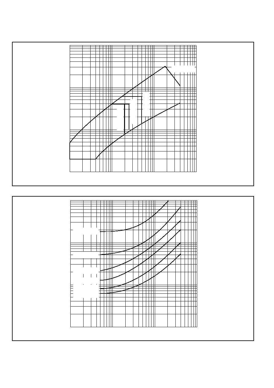
1.0
10
100
1000
Pulse width t
p
- (
µ
s)
1.0
10
100
1000
Energy per pulse - (mJ)
I
TM
= 2000A
I
TM
= 1000A
I
TM
= 600A
I
TM
= 400A
I
TM
= 200A
I
TM
= 100A
0.01
0.1
1.0
10
Gate trigger current I
GT
- (A)
0.1
1.0
10
100
Gate trigger voltage V
GT
- (V)
T
j
= +125∞C
T
j
= +25∞C
T
j
= -40∞C
P
GM
= 50W
Fig.5 Gate characteristics
Fig.6 Sinusoidal energy per pulse (thyristor only)
MAS110S
7/9
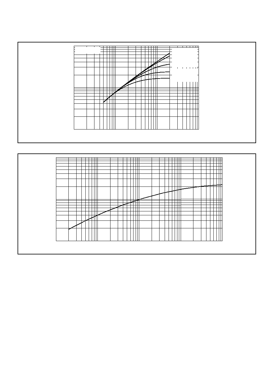
1.0
10
100
1000
Rate of rise of reverse current dI
RR
/dt - (A/
µ
s)
1.0
10
100
Recovered charge Q
R
- (C)
T
j
= 125∞C
I
FM
= 400A
I
FM
= 200A
I
FM
= 100A
I
FM
= 60A
I
FM
= 40A
0.001
0.01
0.1
1.0
Time - (s)
0.01
0.1
1.0
Thermal impedance - (∞C/W)
10
Fig.7 Recovered charge (diode only)
Fig.8 Maximum (limit) transient thermal impedance (thyristor only)
MAS110S
8/9
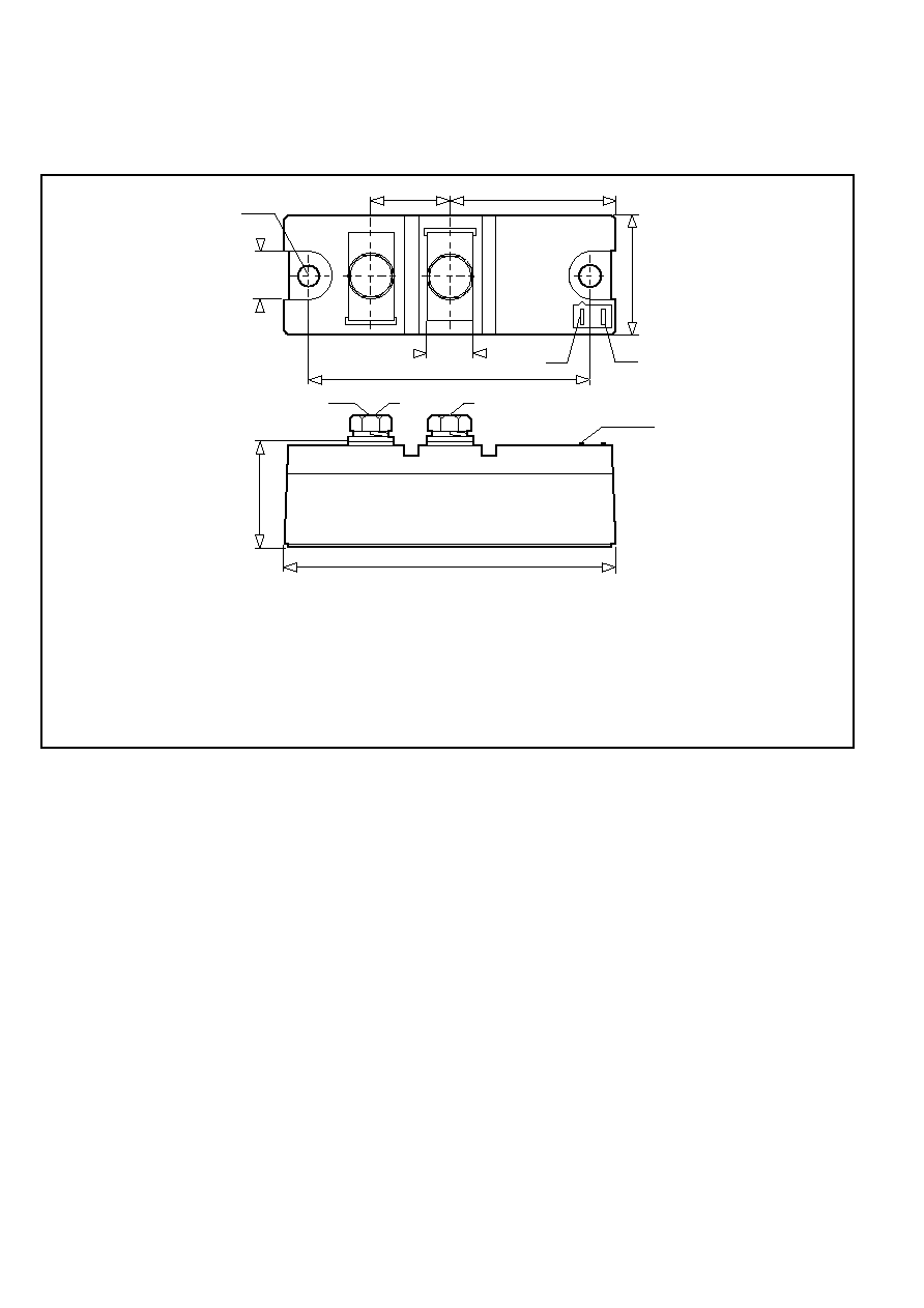
PACKAGE DETAILS
For further package information, please contact your local Customer Service Centre. All dimensions in mm, unless stated otherwise.
DO NOT SCALE.
Recommended fixings for mounting:
M6 socket head cap screws.
Recommended mounting torque:
6Nm (55lb.ins)
Recommended torque for electrical connections:
5Nm (44lb.ins)
Maximum torques for electrical connections:
8Nm (70lb.ins)
Nominal weight:
350g
Module outline type code: MP02
23
47
13
80
34
30
94
M6
ÿ6.5
1
2
K
1
G
1
12.8
2.8x0.8
MAS110S
9/9
POWER ASSEMBLY CAPABILITY
The Power Assembly group was set up to provide a support service for those customers requiring more than the basic semiconduc-
tor, and has developed a flexible range of heatsink / clamping systems in line with advances in device types and the voltage and
current capability of our semiconductors.
We offer an extensive range of air and liquid cooled assemblies covering the full range of circuit designs in general use today. The
Assembly group continues to offer high quality engineering support dedicated to designing new units to satisfy the growing needs of
our customers.
Using the up to date CAD methods our team of design and applications engineers aim to provide the Power Assembly Complete
solution (PACs).
HEATSINKS
Power Assembly has it's own proprietary range of extruded aluminium heatsinks. They have been designed to optimise the
performance or our semiconductors. Data with respect to air natural, forced air and liquid cooling (with flow rates) is available on
request.
For further information on device clamps, heatsinks and assemblies, please contact your nearest Sales Representative or the
factory.
CUSTOMER SERVICE CENTRES
France, Benelux, Italy and Spain Tel: +33 (0)1 69 18 90 00. Fax: +33 (0)1 64 46 54 50
North America Tel: 011-800-5554-5554. Fax: 011-800-5444-5444
UK, Germany, Scandinavia & Rest Of World Tel: +44 (0)1522 500500. Fax: +44 (0)1522 500020
SALES OFFICES
France, Benelux, Italy and Spain Tel: +33 (0)1 69 18 90 00. Fax: +33 (0)1 64 46 54 50
Germany Tel: 07351 827723
North America Tel: (613) 723-7035. Fax: (613) 723-1518. Toll Free: 1.888.33.DYNEX (39639) /
Tel: (831) 440-1988. Fax: (831) 440-1989 / Tel: (949) 733-3005. Fax: (949) 733-2986.
UK, Germany, Scandinavia & Rest Of World Tel: +44 (0)1522 500500. Fax: +44 (0)1522 500020
These offices are supported by Representatives and Distributors in many countries world-wide.
© Dynex Semiconductor 2000 Publication No. DS4200-5 Issue No. 5.0 January 2000
TECHNICAL DOCUMENTATION ≠ NOT FOR RESALE. PRINTED IN UNITED KINGDOM
HEADQUARTERS OPERATIONS
DYNEX SEMICONDUCTOR LTD
Doddington Road, Lincoln.
Lincolnshire. LN6 3LF. United Kingdom.
Tel: 00-44-(0)1522-500500
Fax: 00-44-(0)1522-500550
DYNEX POWER INC.
Unit 7 - 58 Antares Drive,
Nepean, Ontario, Canada K2E 7W6.
Tel: 613.723.7035
Fax: 613.723.1518
Toll Free: 1.888.33.DYNEX (39639)
This publication is issued to provide information only which (unless agreed by the Company in writing) may not be used, applied or reproduced for any purpose nor form part of any order or contract nor to be regarded as
a representation relating to the products or services concerned. No warranty or guarantee express or implied is made regarding the capability, performance or suitability of any product or service. The Company reserves
the right to alter without prior notice the specification, design or price of any product or service. Information concerning possible methods of use is provided as a guide only and does not constitute any guarantee that such
methods of use will be satisfactory in a specific piece of equipment. It is the user's responsibility to fully determine the performance and suitability of any equipment using such information and to ensure that any publication
or data used is up to date and has not been superseded. These products are not suitable for use in any medical products whose failure to perform may result in significant injury
or death to the user. All products and materials are sold and services provided subject to the Company's conditions of sale, which are available on request.
All brand names and product names used in this publication are trademarks, registered trademarks or trade names of their respective owners.
http://www.dynexsemi.com
e-mail: power_solutions@dynexsemi.com
Datasheet Annotations:
Dynex Semiconductor annotate datasheets in the top right hard corner of the front page, to indicate product status. The annotations are as follows:-
Target Information: This is the most tentative form of information and represents a very preliminary specification. No actual design work on the product has been started.
Preliminary Information: The product is in design and development. The datasheet represents the product as it is understood but details may change.
Advance Information: The product design is complete and final characterisation for volume production is well in hand.
No Annotation: The product parameters are fixed and the product is available to datasheet specification.