 | –≠–ª–µ–∫—Ç—Ä–æ–Ω–Ω—ã–π –∫–æ–º–ø–æ–Ω–µ–Ω—Ç: RD33FG04 | –°–∫–∞—á–∞—Ç—å:  PDF PDF  ZIP ZIP |
RD33FG
1/7
www.dynexsemi.com
FEATURES
s
Optimised For High Current Rectifiers
s
High Surge Capability
s
Very Low On-state Voltage
APPLICATIONS
s
Electroplating
s
Power Supplies
s
Welding
VOLTAGE RATINGS
ORDERING INFORMATION
When ordering, select the required part number shown in the
Voltage Ratings selection table.
For example:
RD33FG03
Note: Please use the complete part number when ordering and
quote this number in any future correspondance relating to your
order.
KEY PARAMETERS
V
RRM
600V
I
F(AV)
(max)
3997A
I
FSM
(max)
46750A
RD33FG
Rectifier Diode
Target Information
Replaces November 2000, version DS5415-1.1
DS5415-2.0 October 2001
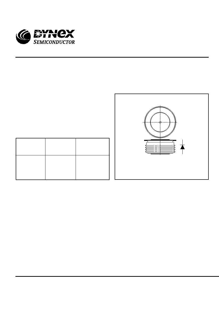
Fig. 1 Package outline
Outline type code: G
(See Package Details for further information)
Conditions
V
RSM
= V
RRM
600
500
400
300
200
100
RD33FG06
RD33FG05
RD33FG04
RD33FG03
RD33FG02
RD33FG01
Part and Ordering
Number
Repetitive Peak
Reverse Voltage
V
RRM
V
RD33FG
2/7
www.dynexsemi.com
Symbol
I
F(AV)
I
F(RMS)
I
F
I
F(AV)
I
F(RMS)
I
F
Test Conditions
Half wave resistive load
-
-
Half wave resistive load
-
-
Units
A
A
A
A
A
A
Max.
3830
6010
6080
2710
4260
4210
Parameter
Mean forward current
RMS value
Continuous (direct) forward current
Mean forward current
RMS value
Continuous (direct) forward current
Single Side Cooled
Double Side Cooled
CURRENT RATINGS
T
case
= 75
o
C unless otherwise stated
Symbol
Parameter
Conditions
Double Side Cooled
I
F(AV)
Mean forward current
I
F(RMS)
RMS value
I
F
Continuous (direct) forward current
Single Side Cooled (Anode side)
I
F(AV)
Mean forward current
I
F(RMS)
RMS value
I
F
Continuous (direct) forward current
Units
Max.
Half wave resistive load
3997
A
-
6278
A
-
6358
A
Half wave resistive load
2831
A
-
4447
A
-
4401
A
T
case
= 85∞C unless otherwise stated
RD33FG
3/7
www.dynexsemi.com
Units
mA
A
µ
C
V
m
Parameter
Thermal resistance - junction to case
Thermal resistance - case to heatsink
Virtual junction temperature
Storage temperature range
Clamping force
Parameter
Surge (non-repetitive) forward current
I
2
t for fusing
Surge (non-repetitive) forward current
I
2
t for fusing
Test Conditions
10ms half sine, T
case
= 175∞C
V
R
= 50% V
RRM
- 1/4 sine
10ms half sine, T
case
= 175∞C
V
R
= 0
Symbol
I
FSM
I
2
t
I
FSM
I
2
t
SURGE RATINGS
Units
kA
A
2
s
kA
A
2
s
Max.
37.4
7.0 x 10
6
46.75
10.93 x 10
6
Test Conditions
At V
RRM
, T
case
= 200∞C
I
F
= 1000A, dI
RR
/dt = 3A/
µ
s,
T
case
= 200∞C, V
R
= 100V
At T
vj
= 200∞C
At T
vj
= 200∞C
Parameter
Peak reverse current
Peak reverse recovery current
Total stored charge
Threshold voltage
Slope resistance
CHARACTERISTICS
Symbol
I
RM
I
rr
Q
S
V
TO
r
T
Max.
50
30
160
0.6
0.0872
Min.
-
-
-
-
-
Test Conditions
Double side cooled
DC
Single side cooled
Anode DC
Cathode DC
Clamping force 12.0kN
Double side
(with mounting compound)
Single side
Forward (conducting)
Reverse (blocking)
THERMAL AND MECHANICAL RATINGS
Symbol
R
th(j-c)
R
th(c-h)
T
vj
T
stg
F
m
Units
∞CW
∞CW
∞CW
∞CW
∞CW
∞C
∞C
∞C
kN
Max.
0.032
0.064
0.064
0.008
0.016
225
200
200
13.2
Min.
-
-
-
-
-
-
-
≠55
10.8

RD33FG
4/7
www.dynexsemi.com
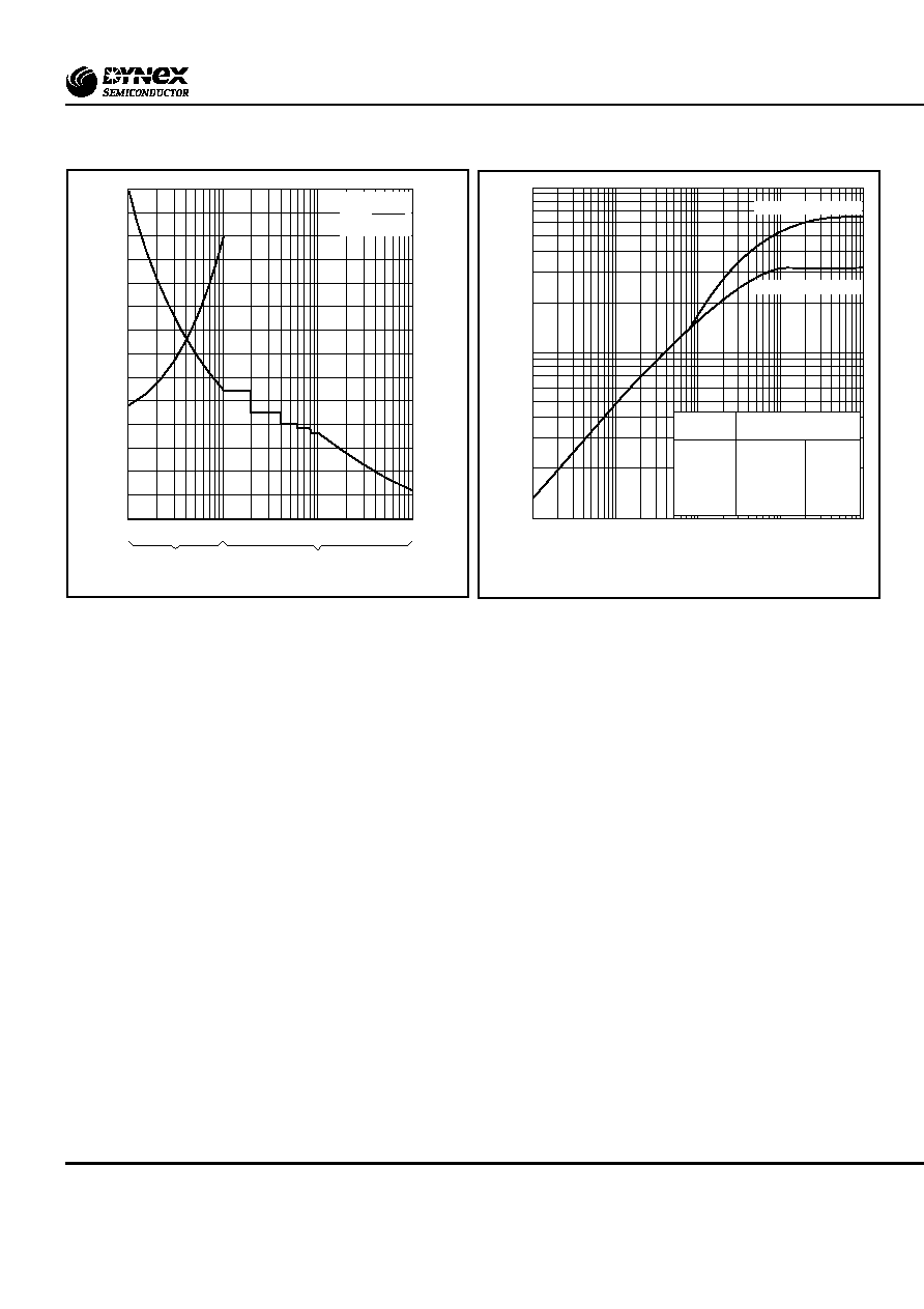
CURVES
Fig. 2 Maximum (limit) forward characteristics
Fig. 3 Power dissipation
Fig. 4 Maximum stored charge and reverse recovery current vs dI/dt
0
500
1000
1500
2000
2500
3000
0.5
0.55
0.6
0.65
0.7
0.75
0.8
0.85
0.9
Instantaneous forward voltage, V
F
- (V)
Instantaneous forward current, I
F
- (A)
T
j
= 200∞C
0
1000
2000
3000
4000
0
500
1000
1500
2000
2500
3000
3500
4000
Mean forward current, I
F(AV)
- (A)
Mean power dissipation - (W)
dc
1/2 wave
3 phase
6 phase
0.1
1.0
10
100
Rate of decay of forward current, dI
F
/dt - (A/µs)
1000
100
10
Stored charge Q
S
- (µ
C)
Conditions:
T
j
= 200∞C
V
R
= 100V
I
F
= 2000A
I
RM
Q
S
I
F
dI/dt
1000
100
10
Reverse recovery current I
RR
- (A)
Max. Q
S
Max. I
RR
RD33FG
5/7
www.dynexsemi.com
Fig. 6 Maximum (limit) transient thermal impedance
Fig. 5 Surge (non-repetitive) forward current vs time
(with 50% V
RRM
@ T
case
= 175∞C)
1
10
1
2 3 5
10
20
50
10
20
30
40
50
60
80
70
3
4
2
1
5
6
7
8
I
2
t value - (A
2
s x 10
6
)
ms
Cycles at 50Hz
Duration
Peak half sine forward current - (kA)
I
2
t = Œ
2
x t
2
I
2
t
0.1
0.01
0.001
Thermal Impedance - Junction to case (
∞
C/W)
0.001
0.01
0.1
1.0
10
Time - (s)
Double side cooled
Anode side cooled
Conduction
d.c.
Halfwave
3 phase 120∞
6 phase 60∞
Effective thermal resistance
Junction to case ∞C/W
Double side
0.032
0.034
0.044
0.057
Anode side
0.064
0.066
0.076
0.089