 | –≠–ª–µ–∫—Ç—Ä–æ–Ω–Ω—ã–π –∫–æ–º–ø–æ–Ω–µ–Ω—Ç: P4KE400 | –°–∫–∞—á–∞—Ç—å:  PDF PDF  ZIP ZIP |
P4KE SERIES
TRANSIENT VOLTAGE
SUPPRESSOR
V
BR
: 6.8 - 440 Volts
P
PK
: 400 Watts
FEATURES :
* 400W surge capability at 1ms
* Excellent clamping capability
* Low zener impedance
* Fast response time : typically less
then 1.0 ps from 0 volt to V
BR(min.)
* Typical I
R
less then 1 A above 10V
MECHANICAL DATA
* Case : DO-41 Molded plastic
* Epoxy : UL94V-O rate flame retardant
* Lead : Axial lead solderable per MIL-STD-202,
method 208 guaranteed
* Polarity : Color band denotes cathode end except Bipolar.
* Mounting position : Any
* Weight : 0.339 gram
DEVICES FOR BIPOLAR APPLICATIONS
For bi-directional use C or CA Suffix
Electrical characteristics apply in both directions
MAXIMUM RATINGS
Peak Power Dissipation at Ta = 25 ∞C, Tp=1ms (Note1)
PPK
Minimum 400
Watts
Steady State Power Dissipation at TL = 75 ∞C
Lead Lengths 0.375", (9.5mm) (Note 2)
PD
1.0
Watt
Peak Forward Surge Current, 8.3ms Single Half
Sine-Wave Superimposed on Rated Load
(JEDEC Method) (Note 3)
IFSM
40
Amps.
Operating and Storage Temperature Range
TJ, TSTG
- 65 to + 175
∞C
Note :
Dimensions in inches and (millimeters)
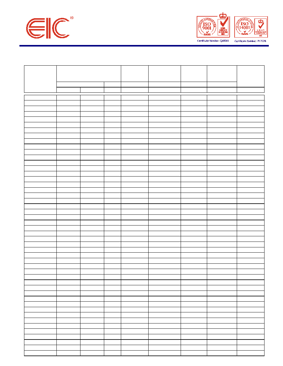
ELECTRICAL CHARACTERISTICS
Rating at = 25
∞
C ambient temperature unless otherwise specified
Breakdown Voltage @ It
Working Peak
Maximum
Maximum
Maximum
Maximum
( Note 1 )
Reverse
Reverse Leakage
Reverse
Clamping
Temperature
TYPE
Voltage
@ V
RWM
Current
Voltage @ I
RSM
Co-efficient
V
BR
(V)
It
V
RWM
I
R
I
RSM
V
RSM
of V
BR
Min.
Max.
(mA)
(V)
( A)
(A)
(V)
(% /
∞
C)
P4KE6.8
6.12
7.48
10
5.50
1000
38.0
10.8
0.057
P4KE6.8A
6.45
7.14
10
5.80
1000
40.0
10.5
0.057
P4KE7.5
6.75
8.25
10
6.05
500
36.0
11.7
0.061
P4KE7.5A
7.13
7.88
10
6.40
500
37.0
11.3
0.061
P4KE8.2
7.38
9.02
10
6.63
200
33.0
12.5
0.065
P4KE8.2A
7.79
8.61
10
7.02
200
35.0
12.1
0.065
P4KE9.1
8.19
10.0
1.0
7.37
50
30.0
13.8
0.068
P4KE9.1A
8.65
9.55
1.0
7.78
50
31.0
13.4
0.068
P4KE10
9.00
11.0
1.0
8.10
10
28.0
15.0
0.073
P4KE10A
9.50
10.5
1.0
8.55
10
29.0
14.5
0.073
P4KE11
9.90
12.1
1.0
8.92
5.0
26.0
16.2
0.075
P4KE11A
10.5
11.6
1.0
9.40
5.0
27.0
15.6
0.075
P4KE12
10.8
13.2
1.0
9.72
5.0
24.0
17.3
0.078
P4KE12A
11.4
12.6
1.0
10.2
5.0
25.0
16.7
0.078
P4KE13
11.7
14.3
1.0
10.5
5.0
22.0
19.0
0.081
P4KE13A
12.4
13.7
1.0
11.1
5.0
23.0
18.2
0.081
P4KE15
13.5
16.5
1.0
12.1
5.0
19.0
22.0
0.084
P4KE15A
14.3
15.8
1.0
12.8
5.0
20.0
21.2
0.084
P4KE16
14.4
17.6
1.0
12.9
5.0
18.0
23.5
0.086
P4KE16A
15.2
16.8
1.0
13.6
5.0
19.0
22.5
0.086
P4KE17
15.3
18.7
1.0
13.7
5.0
17.0
25.0
0.087
P4KE17A
16.2
17.9
1.0
14.5
5.0
18.0
24.0
0.087
P4KE18
16.2
19.8
1.0
14.5
5.0
16.0
26.5
0.088
P4KE18A
17.1
18.9
1.0
15.3
5.0
17.0
25.5
0.088
P4KE20
18.0
22.0
1.0
16.2
5.0
14.0
29.1
0.090
P4KE20A
19.0
21.0
1.0
17.1
5.0
15.0
27.7
0.090
P4KE22
19.8
24.2
1.0
17.8
5.0
13.0
31.9
0.092
P4KE22A
20.9
23.1
1.0
18.8
5.0
14.0
30.6
0.092
P4KE24
21.6
26.4
1.0
19.4
5.0
12.0
34.7
0.094
P4KE24A
22.8
25.2
1.0
20.5
5.0
13.0
33.2
0.094
P4KE27
24.3
29.7
1.0
21.8
5.0
11.0
39.1
0.096
P4KE27A
25.7
28.4
1.0
23.1
5.0
11.2
37.5
0.096
P4KE30
27.0
33.0
1.0
24.3
5.0
10.0
43.5
0.097
P4KE30A
28.5
31.5
1.0
25.6
5.0
10.0
41.4
0.097
P4KE33
29.7
36.3
1.0
26.8
5.0
9.0
47.7
0.098
P4KE33A
31.4
34.7
1.0
28.2
5.0
9.0
45.7
0.098
P4KE36
32.4
39.6
1.0
29.1
5.0
8.0
52.0
0.099
P4KE36A
34.2
37.8
1.0
30.8
5.0
8.4
49.9
0.099
P4KE39
35.1
42.9
1.0
31.6
5.0
7.4
56.4
0.100
P4KE39A
37.1
41.0
1.0
33.3
5.0
7.8
53.9
0.100
P4KE43
38.7
47.3
1.0
34.8
5.0
6.8
61.9
0.101
P4KE43A
40.9
45.2
1.0
36.8
5.0
7.1
59.3
0.101
P4KE47
42.3
51.7
1.0
38.1
5.0
6.2
67.8
0.101
P4KE47A
44.7
49.4
1.0
40.2
5.0
6.5
64.8
0.101
P4KE51
45.9
56.1
1.0
41.3
5.0
5.7
73.5
0.102
P4KE51A
48.5
53.6
1.0
43.6
5.0
6.0
70.1
0.102
P4KE56
50.4
61.6
1.0
45.4
5.0
5.2
80.5
0.103
P4KE56A
53.2
58.8
1.0
47.8
5.0
5.5
77.0
0.103
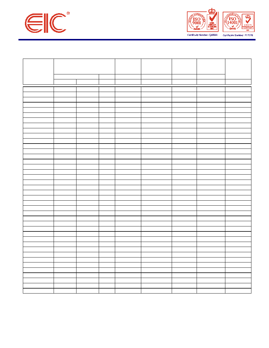
ELECTRICAL CHARACTERISTICS
Rating at = 25
∞
C ambient temperature unless otherwise specified
Breakdown Voltage @ It
Working Peak
Maximum
Maximum
Maximum
Maximum
( Note 1 )
Reverse
Reverse Leakage
Reverse
Clamping
Temperature
TYPE
Voltage
@ V
RWM
Current
Voltage @ I
RSM
Co-efficient
V
BR
(V)
It
V
RWM
I
R
I
RSM
V
RSM
of V
BR
Min.
Max.
(mA)
(V)
( A)
(A)
(V)
(% /
∞
C)
P4KE62
55.8
68.2
1.0
50.2
5.0
4.7
89.0
0.104
P4KE62A
58.9
65.1
1.0
53.0
5.0
5.0
85.0
0.104
P4KE68
61.2
74.8
1.0
55.1
5.0
4.3
98.0
0.104
P4KE68A
64.6
71.4
1.0
58.1
5.0
4.6
92.0
0.104
P4KE75
67.5
82.5
1.0
60.7
5.0
3.9
108
0.105
P4KE75A
71.3
78.8
1.0
64.1
5.0
4.1
103
0.105
P4KE82
73.8
90.2
1.0
66.4
5.0
3.6
118
0.105
P4KE82A
77.9
86.1
1.0
70.1
5.0
3.7
113
0.105
P4KE91
81.9
100
1.0
73.7
5.0
3.2
131
0.106
P4KE91A
86.5
95.5
1.0
77.8
5.0
3.4
125
0.106
P4KE100
90.0
110
1.0
81.0
5.0
2.9
144
0.106
P4KE100A
95.0
105
1.0
85.5
5.0
3.1
137
0.106
P4KE110
99.0
121
1.0
89.2
5.0
2.7
158
0.107
P4KE110A
105
116
1.0
94.0
5.0
2.8
152
0.107
P4KE120
108
132
1.0
97.2
5.0
2.4
173
0.107
P4KE120A
114
126
1.0
102
5.0
2.5
165
0.107
P4KE130
117
143
1.0
105
5.0
2.2
187
0.107
P4KE130A
124
137
1.0
111
5.0
2.3
179
0.107
P4KE150
135
165
1.0
121
5.0
2.0
215
0.108
P4KE150A
143
158
1.0
128
5.0
2.0
207
0.108
P4KE160
144
176
1.0
130
5.0
1.8
230
0.108
P4KE160A
152
168
1.0
136
5.0
1.9
219
0.108
P4KE170
153
187
1.0
138
5.0
1.7
244
0.108
P4KE170A
162
179
1.0
145
5.0
1.8
234
0.108
P4KE180
162
198
1.0
146
5.0
1.6
258
0.108
P4KE180A
171
189
1.0
154
5.0
1.7
246
0.108
P4KE200
180
220
1.0
162
5.0
1.5
287
0.108
P4KE200A
190
210
1.0
171
5.0
1.53
274
0.108
P4KE220
198
242
1.0
175
5.0
1.16
344
0.108
P4KE220A
209
231
1.0
185
5.0
1.22
328
0.108
P4KE250
225
275
1.0
202
5.0
1.11
360
0.110
P4KE250A
237
263
1.0
214
5.0
1.16
344
0.110
P4KE300
270
330
1.0
243
5.0
0.93
430
0.110
P4KE300A
285
315
1.0
256
5.0
0.97
414
0.110
P4KE350
315
385
1.0
284
5.0
0.79
504
0.110
P4KE350A
332
368
1.0
300
5.0
0.83
482
0.110
P4KE400
360
440
1.0
324
5.0
0.70
574
0.110
P4KE400A
380
420
1.0
342
5.0
0.73
548
0.110
P4KE440
396
484
1.0
356
5.0
0.95
631
0.110
P4KE440A
418
462
1.0
376
5.0
1.00
602
0.110
( 1 ) V
BR
measured after It applied for 300 s., It = square wave pulse or equivalent.
( 2 ) V
F
= 3.5 Vmax., I
F
= 25 Amps. ( 6.8 Volts thru 91Volts )
V
F
= 5.0 Vmax., I
F
= 25 Amps. ( 100 Volts thru 440 Volts ) per 1/2 square or equivalent sine wave.
PW = 8.3 ms, duty cycle = 4 pulses per minute maximum.
( 3 ) For Bipolar types having V
R
of 10 Volts and under, the I
R
limit is doubled.
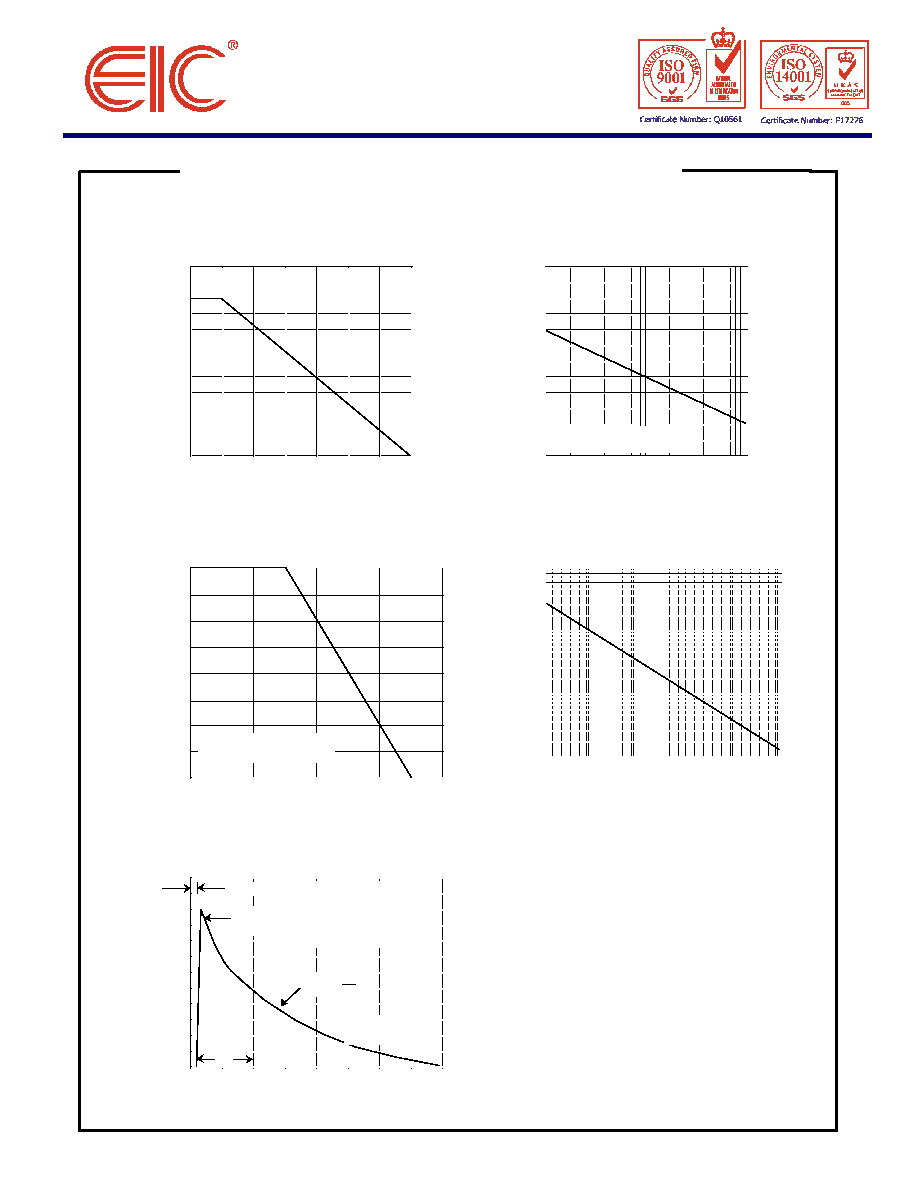
RATING AND CHARACTERISTIC CURVES ( P4KE SERIES )
FIG.1 - PULSE DERATING CURVE
FIG.2 - MAXIMUM NON-REPETITIVE
SURGE CURRENT
0
25
50
75
100
125
150
175
Ta, AMBIENT TEMPERATURE, (
∞
C)
NUMBER OF CYCLES AT 60Hz
FIG.3 - STEADY STATE POWER DERATING
FIG.4 - PULSE RATING CURVE
FIG.5 - PULSE WAVEFORM
0
1.0
2.0
3.0
4.0
80
60
40
20
120
1.00
100
10
40
0
60
0
30
20
10
0.25
0.75
0
0.1
0.50
1.0
tp, PULSE WIDTH
PEAK FORWARD SURGE
CURRENT, AMPERES
PEAK PULSE DERATING IN % OF
PEAK POWER OR CURRENT
Pp,PEAK POWER (kW)
100
50
10
20
60
1
2
4
6
40
100
100
125
175
0
25
50
75
150
0.1ms
1.0ms
10ms
100ms
10ms
1.0ms
200
T
L
, LEAD TEMPERATURE (
∞
C)
P
D
, STEADY STATE POWER DISSIPATION
(WATTS)
50
100
0
Tr = 10ms
Peak Value
IRMS
Half Value - IRMS
2
TJ=25 ∞C
Pulse Width (tp) is defined
as that point where the peak
current decays to 50%
of IRSM
tp
10X1000 Waveform
as defined by R.E.A.
T, TIME(ms)
PEAK PULSE CURRENT - % I
RMS
Single Phase Half Wave
60 Hz Resistive or Inductive load
8.3 ms SINGLE HALF SINE WAVE
JEDEC METHOD