 | –≠–ª–µ–∫—Ç—Ä–æ–Ω–Ω—ã–π –∫–æ–º–ø–æ–Ω–µ–Ω—Ç: EL2002CM | –°–∫–∞—á–∞—Ç—å:  PDF PDF  ZIP ZIP |

EL2002C
December
1995
Rev
D
EL2002C
Low Power 180 MHz Buffer Amplifier
Note All information contained in this data sheet has been carefully checked and is believed to be accurate as of the date of publication however this data sheet cannot be a ``controlled document'' Current revisions if any to these
specifications are maintained at the factory and are available upon your request We recommend checking the revision level before finalization of your design documentation
1989 Elantec Inc
Features
180 MHz bandwidth
2000 V ms slew rate
Low bias current 3 mA typical
100 mA output current
5 mA supply current
Short circuit protected
Low cost
Stable with capacitive loads
Wide supply range
g
5V to
g
15V
No thermal runaway
Applications
Op amp output current booster
Cable line driver
A D input buffer
Isolation buffer
Ordering Information
Part No
Temp Range
Package
Outline
EL2002ACN
0 C to
a
75 C
P-DIP
MDP0031
EL2002CM
0 C to
a
75 C
20-Lead SOL
MDP0027
EL2002CN
0 C to
a
75 C
P-DIP
MDP0031
General Description
The EL2002 is a low cost monolithic high slew rate buffer
amplifier Built using the Elantec monolithic Complementary
Bipolar process this patented buffer has a
b
3 dB bandwidth of
180 MHz and delivers 100 mA yet draws only 5 mA of supply
current It typically operates from
g
15V power supplies but
will work with as little as
g
5V
This high speed buffer may be used in a wide variety of applica-
tions in military video and medical systems Typical examples
include fast op-amp output current boosters coaxial cable driv-
ers and A D converter input buffers
Elantec's products and facilities comply with MIL-I-45208A
and other applicable quality specifications For information on
Elantec's processing see the Elantec document QRA-1 Elan-
tec's Processing Monolithic Integrated Circuits
Connection Diagrams
EL2002 DIP Pinout
2002 ≠ 1
Top View
EL2002 SOL Pinout
2002 ≠ 2
Top View
Manufactured Under U S Patent No 4 833 424 and U K Patent No 2217134

EL2002C
Low Power 180 MHz Buffer Amplifier
Absolute Maximum Ratings
V
S
Supply Voltage (V
a
b
V
b
)
g
18V or 36V
V
IN
Input Voltage (Note 1)
g
15V or V
S
I
IN
Input Current (Note 1)
g
50 mA
P
D
Power Dissipation (Note 2)
See Curves
Output Short Circuit
Duration (Note 3)
Continuous
T
A
Operating Temperature Range
EL2002AC EL2002C
0 C to
a
75 C
T
J
Operating Junction Temperature
150 C
T
ST
Storage Temperature
b
65 C to
a
150 C
Important Note
All parameters having Min Max specifications are guaranteed The Test Level column indicates the specific device testing actually
performed during production and Quality inspection Elantec performs most electrical tests using modern high-speed automatic test
equipment specifically the LTX77 Series system Unless otherwise noted all tests are pulsed tests therefore T
J
e
T
C
e
T
A
Test Level
Test Procedure
I
100% production tested and QA sample tested per QA test plan QCX0002
II
100% production tested at T
A
e
25 C and QA sample tested at T
A
e
25 C
T
MAX
and T
MIN
per QA test plan QCX0002
III
QA sample tested per QA test plan QCX0002
IV
Parameter is guaranteed (but not tested) by Design and Characterization Data
V
Parameter is typical value at T
A
e
25 C for information purposes only
Electrical Characteristics
V
S
e
g
15V R
S
e
50
X unless otherwise specified
Parameter
Description
Test Conditions
Limits
EL2002AC
Units
EL2002C
V
IN
Load
Temp
Min
Typ
Max
Test
Level
V
OS
Offset Voltage
0
%
25 C
b
15
5
a
15
I
mV
EL2002A EL2002AC
T
MIN
T
MAX
b
20
a
20
III
mV
EL2002 EL2002C
0
%
25 C
b
40
10
a
40
I
mV
T
MIN
T
MAX
b
50
a
50
III
mV
I
IN
Input Current
0
%
25 C
b
10
3
a
10
I
mA
EL2002A EL2002AC
T
MIN
T
MAX
b
15
a
15
III
mA
EL2002 EL2002C
0
%
25 C
b
15
5
a
15
I
mA
T
MIN
T
MAX
b
20
a
20
III
mA
R
IN
Input Resistance
a
12V
100
X
25 C
1
3
I
M
X
T
MIN
T
MAX
0 1
III
M
X
A
V1
Voltage Gain
g
12V
%
25 C
0 990
0 998
I
V V
T
MIN
T
MAX
0 985
III
V V
A
V2
Voltage Gain
g
10V
100
X
25 C
0 85
0 93
I
V V
T
MIN
T
MAX
0 83
III
V V
2
TD
is
33in

EL2002C
Low Power 180 MHz Buffer Amplifier
Electrical Characteristics
V
S
e
g
15V R
S
e
50
X unless otherwise specified
Contd
Parameter
Description
Test Conditions
Limits
EL2002AC
Units
EL2002C
V
IN
Load
Temp
Min
Typ
Max
Test
Level
A
V3
Voltage Gain
g
3V
100
X
25 C
0 83
0 91
I
V V
with V
S
e
g
5V
T
MIN
T
MAX
0 80
III
V V
V
O
Output Voltage Swing
g
12V
100
X
25 C
g
10
g
11
I
V
T
MIN
T
MAX
g
9 5
III
V
R
OUT
Output Resistance
g
2V
100
X
25 C
8
13
I
X
T
MIN
T
MAX
15
III
X
I
OUT
Output Current
g
12V
(Note 4)
25 C
a
100
a
160
I
mA
T
MIN
T
MAX
g
95
III
mA
I
S
Supply Current
0
%
25 C
5
7 5
II
mA
T
MIN
T
MAX
10
III
mA
PSRR
Supply Rejection
0
%
25 C
60
75
I
dB
(Note 5)
T
MIN
T
MAX
50
III
dB
t
r
Rise Time
0 5V
100
X
25 C
2 8
V
ns
t
d
Propagation Delay
0 5V
100
X
25 C
1 5
V
ns
SR
Slew Rate (Note 6)
g
10V
100
X
25 C
1200
2000
IV
V
ms
Note 1 If the input exceeds the ratings shown (or the supplies) or if the input to output voltage exceeds
g
7 5V then the input
current must be limited to
g
50 mA See the applications section for more information
Note 2 The maximum power dissipation depends on package type ambient temperature and heat sinking See the characteristic
curves for more details
Note 3 A heat sink is required to keep the junction temperature below the absolute maximum when the output is short circuited
Note 4 Force the input to
a
12V and the output to
a
10V and measure the output current Repeat with
b
12 V
IN
and
b
10V on the
output
Note 5 V
OS
is measured at V
S
a
e
a
4 5V V
S
b
e
b
4 5V and V
S
a
e
a
18V V
S
b
e
18V Both supplies are changed
simultaneously
Note 6 Slew rate is measured between V
OUT
e a
5V and
b
5V
3
TD
is
35in
EL2002C
Low Power 180 MHz Buffer Amplifier
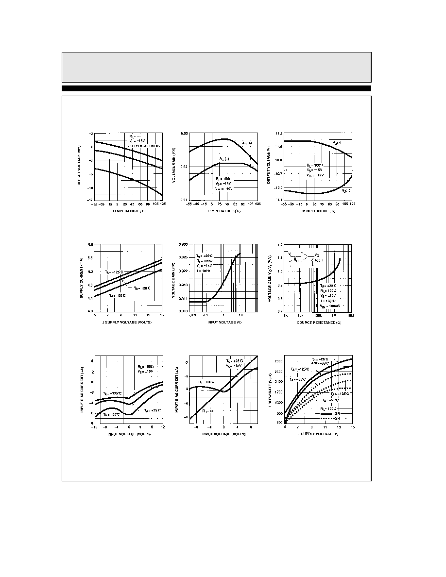
Typical Performance Curves
vs Temperature
Offset Voltage
vs Temperature
Voltage Gain
vs Temperature
Output Voltage Swing
vs Supply Voltage
Supply Current
vs Input Voltage
Voltage Gain
vs Source Resistance
Voltage Gain
at Various Temperatures
vs Input Voltage
Input Bias Current
vs Input Voltage
Input Bias Current
Supply Voltage
g
Slew Rate vs
2002 ≠ 4
4
EL2002C
Low Power 180 MHz Buffer Amplifier
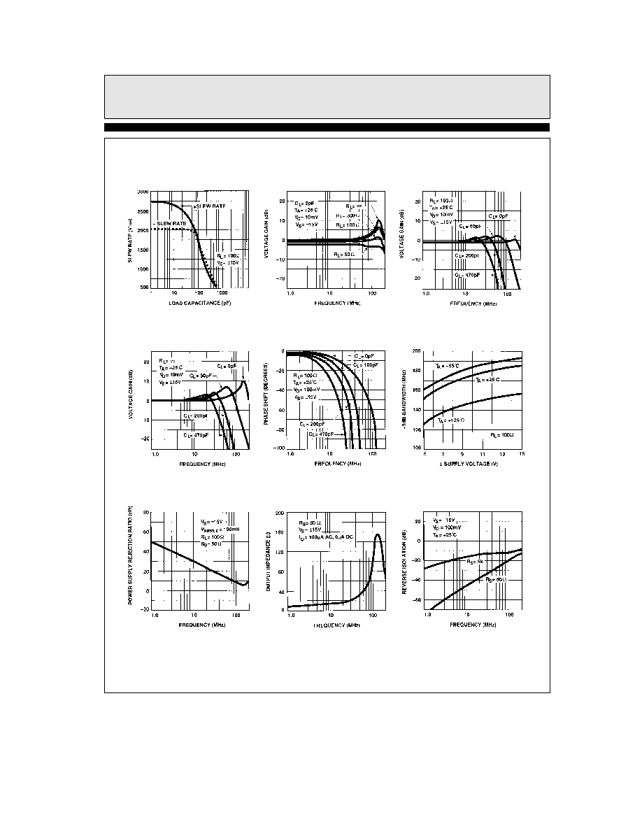
Typical Performance Curves
Contd
vs Load Capacitance
Slew Rate
for Various Resistive Loads
Voltage Gain vs Frequency
Capacitive Loads R
L
e
100X
vs Frequency for Various
Voltage Gain
Capacitive Loads R
L
e
%
vs Frequency for Various
Voltage Gain
for Various Capacitive Loads
Phase Shift vs Frequency
vs Supply Voltage
b
3 dB Bandwidth
vs Frequency
Power Supply Rejection Ratio
Output Impedance vs Frequency
Reverse Isolation vs Frequency
2002 ≠ 5
5