 | –≠–ª–µ–∫—Ç—Ä–æ–Ω–Ω—ã–π –∫–æ–º–ø–æ–Ω–µ–Ω—Ç: EL2004 | –°–∫–∞—á–∞—Ç—å:  PDF PDF  ZIP ZIP |
EL2004EL2004C
November
1993
Rev
G
EL2004 EL2004C
350 MHz FET Buffer
Note All information contained in this data sheet has been carefully checked and is believed to be accurate as of the date of publication however this data sheet cannot be a ``controlled document'' Current revisions if any to these
specifications are maintained at the factory and are available upon your request We recommend checking the revision level before finalization of your design documentation Patent pending
1989 Elantec Inc
Features
Slew rate
2500 V
ms
Rise time
1 ns
Bandwidth
350 MHz
ELH0033
pin compatible
g
5 to
g
15V operation
100 mA output current
MIL-STD-883B Rev C devices
manufactured in U S A
Applications
Coaxial cable driver
Fast op amp booster
Flash converter driver
Video line driver
High-speed sample and hold
Pulse transformer driver
A T E pin driver
Ordering Information
Part No
Temp Range
Package Outline
EL2004CG
b
25 C to
a
85 C
TO-8
MDP0002
EL2004G
b
55 C to
a
125 C
TO-8
MDP0002
EL2004L
b
55 C to
a
125 C 52-Pad LCC MDP0013
EL2004L MIL
b
55 C to
a
125 C 52-Pad LCC MDP0013
5962-89659 is the SMD version of this device
Connection Diagram
Case is Electrically Isolated
2004 ≠ 1
Top View
General Description
The EL2004 is a very high-speed FET input buffer line driver
designed for unity gain applications at both high current (up to
100 mA) and at frequencies up to 350 MHz The 2500 V
ms slew
rate and wide bandwidth ensures the stability of the circuit
when the EL2004 is used inside op amp feedback loops
Applications for the EL2004 include line drivers video buffers
wideband instrumentation and high-speed drivers for inductive
and capacitive loads The performance of the EL2004 makes it
an ideal buffer for video applications including input buffers for
flash A D converters and output buffers for video DACs Its
excellent phase linearity is particularly advantageous in digital
signal processing applications
Elantec facilities comply with MIL-I-45208A and are MIL-
STD-1772 certified
Elantec's Military devices comply with
MIL-STD-883B Revision C and are manufactured in our rigidly
controlled ultra-clean facilities in Milpitas California For ad-
ditional information on Elantec's Quality and Reliability Assur-
ance Policy and procedures request brochure QRA-1
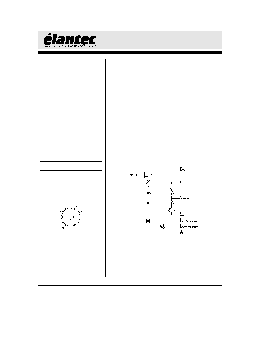
Simplified Schematic
2004 ≠ 3

EL2004 EL2004C
350 MHz FET Buffer
Absolute Maximum Ratings
(T
A
e
25 C)
V
S
Supply Voltage (V
a b
V
b
)
40V
V
IN
Input Voltage
40V
P
D
Power Dissipation (See curves)
1 5W
I
OC
Continuous Output Current
g
100 mA
I
OP
Peak Output Current
g
250 mA
T
A
Operating Temperature Range
EL2004
b
55 C to
a
125 C
EL2004C
b
25 C to
a
85 C
T
J
Operating Junction Temperature
175 C
T
ST
Storage Temperature
b
65 C to
a
150 C
Lead Temperature
(Soldering 10 seconds)
300 C
Important Note
All parameters having Min Max specifications are guaranteed The Test Level column indicates the specific device testing actually
performed during production and Quality inspection Elantec performs most electrical tests using modern high-speed automatic test
equipment specifically the LTX77 Series system Unless otherwise noted all tests are pulsed tests therefore T
J
e
T
C
e
T
A
Test Level
Test Procedure
I
100% production tested and QA sample tested per QA test plan QCX0002
II
100% production tested at T
A
e
25 C and QA sample tested at T
A
e
25 C
T
MAX
and T
MIN
per QA test plan QCX0002
III
QA sample tested per QA test plan QCX0002
IV
Parameter is guaranteed (but not tested) by Design and Characterization Data
V
Parameter is typical value at T
A
e
25 C for information purposes only
g
15V DC Electrical Characteristics
V
S
e
g
15V T
MIN
k
T
A
k
T
MAX
V
IN
e
0V R
L
e
1 k
X unless otherwise specified (Note 1)
Parameter
Description
Test Conditions
EL2004
EL2004C
Units
Min
Typ
Max
Test
Min
Typ
Max
Test
Level
Level
V
OS
Output Offset
R
S
s
100 k
X T
J
e
25 C
5
10
I
12
20
I
mV
Voltage
R
S
s
100 k
X
15
I
25
III
mV
A
V
Voltage Gain
V
IN
e
g
10V
0 97
0 98
1 0
I
0 96
0 98
1 0
II
V V
R
L
e
100
X V
IN
e
g
10V
0 92
0 95
0 98
I
0 90
0 95
0 98
II
V V
R
IN
Input Impedance
T
J
e
25 C V
IN
e
g
1V
10
8
10
11
I
10
8
10
11
I
X
R
OUT
Output
V
IN
e
g
1 V
DC
4
8
I
4
10
II
X
Impedance
DR
L
e
100
X to Infinity
V
O
Output Voltage
V
IN
e
g
14V
g
12
g
13
I
g
12
g
13
II
V
Swing
V
IN
e
g
10 5V R
L
e
100
X
g
9
g
9 8
I
g
9
g
9 8
I
V
T
A
e
25 C
I
IN
Input Current
T
J
e
25 C (Note 2)
0 25
I
2 0
I
nA
T
A
e
25 C (Note 3)
2 5
IV
20
IV
nA
T
J
e
T
A
e
T
MAX
10
I
50
III
nA
V
IN
e b
10V
20
V
20
V
nA
I
S
Supply Current
20
24
I
20
24
II
mA
2
TD
is
32in

EL2004 EL2004C
350 MHz FET Buffer
g
5V DC Electrical Characteristics
V
S
e
g
5V T
MIN
k
T
A
k
T
MAX
V
IN
e
0V R
L
e
50
X unless otherwise specified
Parameter
Description
Test Conditions
EL2004
EL2004C
Units
Min
Typ
Max
Test
Min
Typ
Max
Test
Level
Level
V
OS
Output Offset
R
S
s
100 k
X T
J
e
25 C
10
30
I
10
30
I
mV
Voltage
R
S
s
100 k
X
35
I
35
III
mV
A
V
Voltage Gain
V
IN
e
g
1V R
L
e
1 k
X
0 90
0 95
1 0
I
0 90
0 95
1 0
II
V V
V
IN
e
g
1V
0 80
0 88
0 95
I
0 80
0 88
0 95
II
V V
R
IN
Input Impedance
T
J
e
25 C V
IN
e
g
1V
10
8
10
11
I
10
10
10
11
I
X
R
OUT
Output
V
IN
e
g
1 V
DC
4
8
I
4
10
II
X
Impedance
DR
L
e
50
X to Infinity
V
O
Output Voltage
V
IN
e
g
4V
g
2 0
g
2 9
I
g
2 0
g
2 9
III
V
Swing
I
IN
Input Current
T
J
e
25 C (Note 2)
250
I
500
I
pA
T
A
e
25 C (Note 3)
2 5
IV
5
IV
nA
T
J
e
T
A
e
T
MAX
10
I
20
III
nA
PSRR
Power Supply
V
S
e
g
5V to
g
15V
60
V
60
V
dB
Rejection Ratio
R
L
e
1 k
X
I
S
Supply Current
R
L
e
1 k
X
17 5
20
I
17 5
20
II
mA
Note 1 When operating at elevated temperatures the power dissipation of the EL2004 must be limited to the values shown in the
typical performance curve ``Maximum Power Dissipation vs Temperature'' Junction to case thermal resistance is 31 C W
when dissipation is spread among the transistors in a normal AC steady-state condition In special conditions where heat is
concentrated in one output device junction temperature should be calculated using a thermal resistance of 70 C W
Note 2 Specification is at 25 C junction temperature due to requirements of high-speed automatic testing Actual values at operating
temperatures will exceed the value at T
J
e
25 C When supply voltages are
g
15V no-load operating junction temperatures
may rise 40 C to 60 C above ambient and more under load conditions Accordingly V
OS
may change one to several mV and
I
IN
will change significantly during warm-up Refer to I
IN
vs Temperature graph for expected values
Note 3 Measured in still air seven minutes after application of power See graph of Input Current During Warm-up for further
information
Note 4 Bandwidth is calculated from the rise time The EL2004 has a single pole gain and phase response up to the
b
3 dB
frequency
Note 5 Slew rate is measured between V
OUT
e a
2 5V and
b
2 5V for this test
Note 6 Slew rate is measured between V
OUT
e a
1V and
b
1V for this test Pulse repetition rate is
k
50 MHz
g
15V AC Electrical Characteristics
V
S
e
g
15V R
L
e
1 k
X R
S
e
50
X T
J
e
25 C unless otherwise specified
Parameter
Description
Test Conditions
EL2004
EL2004C
Units
Min
Typ
Max
Test
Min
Typ
Max
Test
Level
Level
BW
Bandwidth
(Note 4)
200
350
I
200
350
I
MHz
R
L
e
50
X
140
200
I
140
200
I
MHz
t
s
Settling Time to 1%
DV
IN
e
1V t
r
e
3 ns
6
V
6
V
ns
C
in
Input Capacitance
3
V
3
V
pF
3
TD
is
32in
TD
is
13in

EL2004 EL2004C
350 MHz FET Buffer
g
15V AC Electrical Characteristics
V
S
e
g
15V R
L
e
1 k
X R
S
e
50
X T
J
e
25 C unless otherwise specified
Contd
Parameter
Description
Test Conditions
EL2004
EL2004C
Units
Min Typ Max
Test
Min Typ Max
Test
Level
Level
SR
Slew Rate
V
IN
e
g
5V (Note 5)
2000
2500
I
2000
2500
I
V
ms
C
L
e
100 pF V
IN
e
g
5V
1200
V
1200
V
V
ms
(Note 5)
t
r
Rise Time
DV
IN
P 0 6V
1 0
1 7
I
1 0
1 7
I
ns
Note See Test Figure
DV
IN
P 0 6V R
L
e
50
X
1 7
2 5
I
1 7
2 5
I
ns
t
p
Propagation Delay
DV
IN
P 0 6V
1 0
2 0
I
1 0
2 0
I
ns
Note See Test Figure
R
OUT
Output
f
e
1 MHz V
IN
e
1 V
RMS
4
V
4
V
X
Impedance
DR
L
e
100
X to Infinity
a
PSRR
Power Supply
DV
S
a e
g
1 5 V
peak
40
V
40
V
dB
Rejection Ratio
f
e
1 kHz
b
PSRR
Power Supply
DV
S
b e
g
1 5 V
peak
40
V
40
V
dB
Rejection Ratio
f
e
1 kHz
g
5V AC Electrical Characteristics
V
S
e
g
5V R
L
e
50
X R
S
e
50
X T
J
e
25 C unless otherwise specified
Parameter
Description
Test Conditions
EL2004
EL2004C
Units
Min Typ Max
Test
Min Typ Max
Test
Level
Level
BW
Bandwidth
R
L
e
1 k
X
175
220
I
175
220
I
MHz
(Note 4)
125
150
IV
125
150
IV
MHz
t
s
Settling Time to 1%
DV
IN
e
1V t
r
e
3 ns
8
V
8
V
ns
C
in
Input Capacitance
3
V
3
V
pF
SR
Slew Rate
V
IN
e
g
2V (Note 6)
900
1200
I
900
1200
I
V
ms
C
L
e
100 pF V
IN
e
g
2V
500
V
500
V
V
ms
R
L
e
1 k
X (Note 6)
t
r
Rise Time
R
L
e
1 k
X DV
IN
P 0 6V
1 6
2 0
I
1 6
2 0
I
ns
Note See Test Figure
R
L
e
50
X DV
IN
P 0 6V
2 3
2 8
IV
2 3
2 8
IV
ns
t
p
Propagation Delay
R
L
e
1 k
X DV
IN
P 0 6V
1 2
2 4
I
1 2
2 4
I
ns
Note See Test Figure
R
OUT
Output
f
e
1 MHz V
IN
e
1 V
RMS
4
V
4
V
X
Impedance
DR
L
e
100
X to Infinity
a
PSRR
Power Supply
DV
S
b e
g
0 5 V
peak
30
V
30
V
dB
Rejection Ratio
f
e
1 kHz
b
PSRR
Power Supply
DV
S
a e
g
0 5 V
peak
30
V
30
V
dB
Rejection Ratio
f
e
1 kHz
4
TD
is
27in
TD
is
34in

EL2004 EL2004C
350 MHz FET Buffer
AC Test Circuit
2004 ≠ 4
Typical Performance Curves
Dissipation
Maximum Power
TO-8
2004 ≠ 5
Gain vs Input Voltage
Output Current
Output Resistance vs
2004 ≠ 7
5